Maximum ratings, Thermal characteristics, Electrical characteristics – Diodes DMN3730UFB4 User Manual
Page 2: A product line of diodes incorporated
DMN3730UFB4
Document number: DS35017 Rev. 5 - 2
2 of 6
July 2013
© Diodes Incorporated
DMN3730UFB4
A Product Line of
Diodes Incorporated
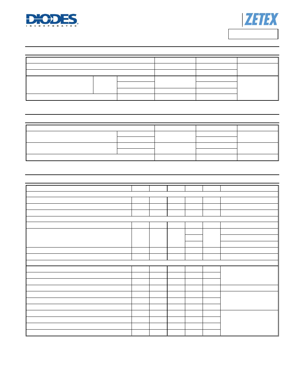
Maximum Ratings
(@T
A
= +25°C, unless otherwise specified.)
Characteristic
Symbol
Value
Unit
Drain-Source Voltage
V
DSS
30
V
Gate-Source Voltage
V
GSS
±8
Continuous Drain Current
V
GS
= 4.5V
(Note 6)
I
D
0.91
A
T
A
= +70°C (Note 6)
0.73
(Note 5)
0.75
Pulsed Drain Current
(Note 7)
I
DM
3
Thermal Characteristics
(@T
A
= +25°C, unless otherwise specified.)
Characteristic Symbol
Value
Unit
Power Dissipation
(Note 6)
P
D
0.69
W
(Note 5)
0.47
Thermal Resistance, Junction to Ambient
(Note 6)
R
θJA
180
°C/W
(Note 5)
258
Operating and Storage Temperature Range
T
J
,
T
STG
-55 to +150
°C
Electrical Characteristics
(@T
A
= +25°C, unless otherwise specified.)
Characteristic
Symbol
Min
Typ
Max
Unit
Test Condition
OFF CHARACTERISTICS
Drain-Source Breakdown Voltage
BV
DSS
30 — — V
V
GS
= 0V, I
D
= 10
μA
Zero Gate Voltage Drain Current
I
DSS
— — 1 µA
V
DS
= 30V, V
GS
= 0V
Gate-Source Leakage
I
GSS
— — 3 µA
V
GS
= ±8V, V
DS
= 0V
ON CHARACTERISTICS
Gate Threshold Voltage
V
GS(th)
0.45 — 0.95 V
V
DS
= V
GS
, I
D
= 250
μA
Static Drain-Source On-Resistance (Note 8)
R
DS(on)
—
—
—
—
—
—
460
m
Ω
V
GS
= 4.5V, I
D
= 200mA
560
V
GS
= 2.5V, I
D
= 100mA
730
V
GS
= 1.8V, I
D
= 75mA
Forward Transfer Admittance
|Y
fs
|
40
— — mS
V
DS
= 3V, I
D
= 10mA
Diode Forward Voltage (Note 8)
V
SD
— 0.7 1.2 V
V
GS
= 0V, I
S
= 300mA
DYNAMIC CHARACTERISTICS (Note 9)
Input Capacitance
C
iss
— 64.3 — pF
V
DS
= 25V, V
GS
= 0V,
f = 1.0MHz
Output Capacitance
C
oss
— 6.1 — pF
Reverse Transfer Capacitance
C
rss
— 4.5 — pF
Gate Resistance
R
g
— 70 —
Ω
V
DS
= 0V, V
GS
= 0V, f = 1MHz
Total Gate Charge
Q
g
— 1.6 — nC
V
GS
= 4.5V, V
DS
= 15V,
I
D
= 1A
Gate-Source Charge
Q
gs
— 0.2 — nC
Gate-Drain Charge
Q
gd
— 0.2 — nC
Turn-On Delay Time
t
D(on)
— 3.5 — ns
V
DS
= 10V, I
D
= 1A
V
GS
= 10V, R
G
= 6Ω
Turn-On Rise Time
t
r
— 2.8 — ns
Turn-Off Delay Time
t
D(off)
— 38 — ns
Turn-Off Fall Time
t
f
— 13 — ns
Notes:
5. For a device surface mounted on a minimum recommended pad layout of an FR4 PCB, in still air conditions; the device is measured when operating in
steady-state condition.
6. Same as note 4, except the device measured at t
10 sec.
7. Same as note 4, except the device is pulsed at duty cycle of 1% for a pulse width of 10
s.
8. Measured under pulsed conditions to minimize self-heating effect. Pulse width
300µs; duty cycle 2%
9. For design aid only, not subject to production testing.