Maximum ratings, Thermal characteristics, Electrical characteristics – Diodes DMN3065LW User Manual
Page 2: Dmn3065lw
DMN3065LW
Document number: DS36078 Rev. 5 - 2
2 of 5
April 2014
© Diodes Incorporated
DMN3065LW
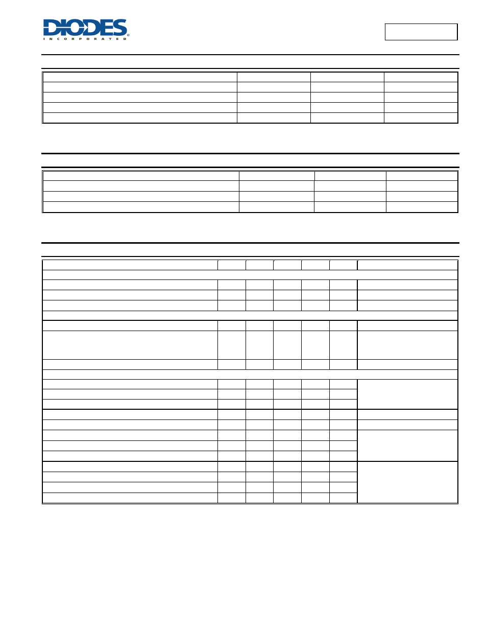
Maximum Ratings
(@T
A
= +25°C, unless otherwise specified.)
Characteristic
Symbol
Value
Unit
Drain Source Voltage
V
DSS
30
V
Gate-Source Voltage
V
GSS
±12
V
Drain Current (Note 5)
I
D
4
A
Body-Diode Continuous Current (Note 5)
I
S
1
A
Thermal Characteristics
Characteristic
Symbol
Value
Unit
Total Power Dissipation (Note 5)
P
D
770 mW
Thermal Resistance, Junction to Ambient @T
A
= +25°C (Note 5)
R
θJA
162 °C/W
Operating and Storage Temperature Range
T
J,
T
STG
-55 to +150
°C
Electrical Characteristics
(@T
A
= +25°C, unless otherwise specified.)
Characteristic
Symbol
Min
Typ
Max
Unit
Test Condition
OFF CHARACTERISTICS (Note 6)
Drain-Source Breakdown Voltage
BV
DSS
30
⎯
⎯
V
V
GS
= 0V, I
D
= 250µA
Zero Gate Voltage Drain Current
I
DSS
⎯
⎯
1
µA
V
DS
= 30V, V
GS
= 0V
Gate-Body Leakage
I
GSS
⎯
⎯
±100
nA
V
GS
= ±12V, V
DS
= 0V
ON CHARACTERISTICS (Note 6)
Gate Threshold Voltage
V
GS(th)
0.5
⎯
1.5
V
V
DS
= V
GS
, I
D
= 250µA
Static Drain-Source On-Resistance
R
DS (ON)
⎯
⎯
⎯
⎯
⎯
52
65
85
mΩ
V
GS
= 10V, I
D
= 4A
V
GS
= 4.5V, I
D
= 3A
V
GS
= 2.5V, I
D
= 2A
Source-Drain Diode Forward Voltage
V
SD
⎯
⎯
1.2 V
V
GS
= 0V, I
S
= 2.0A
DYNAMIC CHARACTERISTICS(7)
Input Capacitance
Ciss
⎯
465
⎯
pF
VDS = 15V, VGS = 0V, f =
1.0MHz
Output Capacitance
Coss
⎯
49.5
⎯
pF
Reverse Transfer Capacitance
Crss
⎯
43.8
⎯
pF
Gate Resistance
R
g
⎯
2.3
⎯
Ω
V
DS
=0V, V
GS
= 0V, f = 1MHz
Total Gate Charge (V
GS
=10V)
Q
g
⎯
11.7
⎯
nC
V
DS
= 15V, I
D
= 4 A
Total Gate Charge (V
GS
=4.5V)
Q
g
⎯
5.5
⎯
nC
V
DS
= 15V, I
D
= 4 A
Gate-Source Charge
Q
gs
⎯
1.1
⎯
nC
Gate-Drain Charge
Q
gd
⎯
1.8
⎯
nC
Turn-On Delay Time
t
D(on)
⎯
1.9
⎯
ns
V
DD
= 15V, V
GEN
= 10V,
R
GEN
=3Ω, R
L
= 3.75Ω
Turn-On Rise Time
t
r
⎯
1.6
⎯
ns
Turn-Off Delay Time
t
D(off)
⎯
10.3
⎯
ns
Turn-Off Fall Time
t
f
⎯
2.0
⎯
ns
Notes:
5. Device mounted on FR-4 substrate PC board, 2oz copper, with 1inch square copper pad layout
6. Short duration pulse test used to minimize self-heating effect.
7.
Guaranteed by design. Not subject to production testing.