Electrical characteristics, Dmn3033ldm – Diodes DMN3033LDM User Manual
Page 2
DMN3033LDM
Document number: DS31345 Rev. 4 - 2
2 of 5
July 2009
© Diodes Incorporated
DMN3033LDM
Electrical Characteristics
@T
A
= 25°C unless otherwise specified
Characteristic Symbol
Min
Typ
Max
Unit
Test
Condition
STATIC CHARACTERISTICS
Drain-Source Breakdown Voltage
BV
DSS
30
⎯
⎯
V
I
D
= 250
μA, V
GS
= 0V
Zero Gate Voltage Drain Current T
J
= 25
°C
T
J
= 55
°C
I
DSS
⎯
⎯
1
5
μA
V
DS
= 30V, V
GS
= 0V
Gate-Body Leakage Current
I
GSS
⎯
⎯
±100
nA
V
DS
= 0V, V
GS
=
±20V
Gate Threshold Voltage
V
GS(th)
1.0
⎯
2.1 V
V
DS
= V
GS
, I
D
= 250
μA
Static Drain-Source On-Resistance (Note 5)
R
DS (ON)
⎯
25
36
33
40
m
Ω
V
GS
= 10V, I
D
= 6.9A
V
GS
= 4.5V, I
D
= 5.0A
Forward Transconductance (Note 5)
g
FS
⎯
5
⎯
S
V
DS
= 10V, I
D
= 8A
Diode Forward Voltage (Note 5)
V
SD
⎯
0.7 1.1 V
I
S
= 2.25A, V
GS
= 0V
DYNAMIC CHARACTERISTICS (Note 6)
Input Capacitance
C
iss
⎯
755
⎯
pF
V
DS
= 10V, V
GS
= 0V
f = 1.0MHz
Output Capacitance
C
oss
⎯
136
⎯
pF
Reverse Transfer Capacitance
C
rss
⎯
108
⎯
pF
Gate Resisitance
R
G
⎯
0.89
⎯
Ω
V
GS
= 0V, V
DS
= 0V, f = 1MHz
SWITCHING CHARACTERISTICS
Total Gate Charge
Q
g
⎯
6.4
13.0
⎯
nC
V
GS
= 4.5V, V
DS
= 15V, I
D
= 5A
V
GS
= 10V, V
DS
= 15V, I
D
= 6.9A
Gate-Source Charge
Q
gs
⎯
1.9
⎯
nC
V
GS
= 10V, V
DS
= 15V, I
D
= 6.9A
Gate-Drain Charge
Q
gd
⎯
3.2
⎯
nC
V
GS
= 10V, V
DS
= 15V, I
D
= 6.9A
Turn-On Delay Time
t
D(on)
⎯
11
⎯
ns
V
DD
= 15V, V
GS
= 10V,
R
D
= 1.8
Ω, R
G
= 6
Ω
Turn-On Rise Time
t
r
⎯
7
⎯
ns
Turn-Off Delay Time
t
D(off)
⎯
63
⎯
ns
Turn-Off Fall Time
t
f
⎯
30
⎯
ns
Notes:
5. Test pulse width t = 300ms.
6. Guaranteed by design. Not subject to production testing.
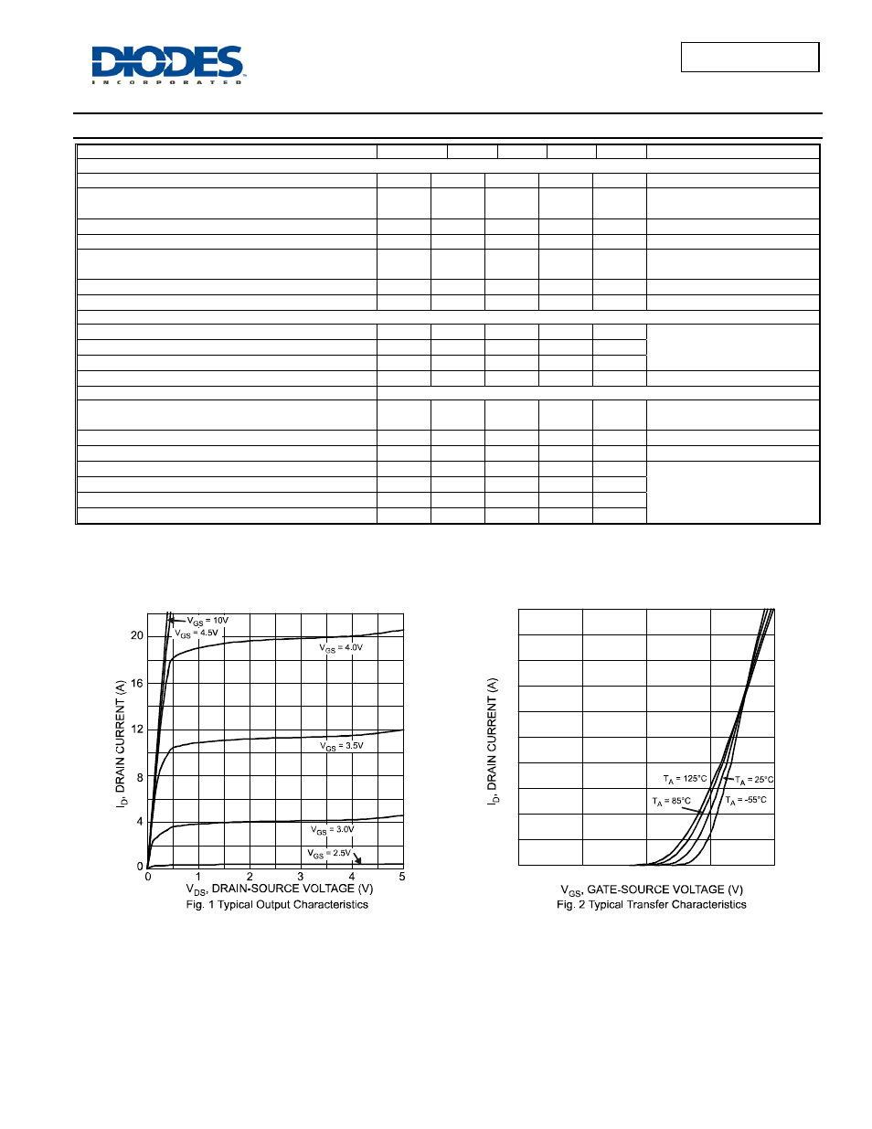
0
2
4
6
8
10
12
14
16
18
20
0
1
2
3
4
V
= 5V
Pulsed
DS