Dmn3025lfg new prod uc t, Maximum ratings, Thermal characteristics – Diodes DMN3025LFG User Manual
Page 2: Electrical characteristics, Dmg3025lfg
POWERDI is a registered trademark of Diodes Incorporated.
DMG3025LFG
Document number: DS35642 Rev. 5 – 2
2 of 6
November 2012
© Diodes Incorporated
DMN3025LFG
NEW PROD
UC
T
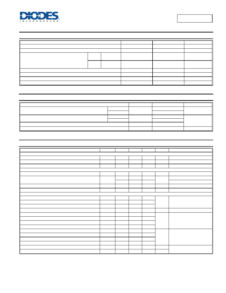
Maximum Ratings
(@T
A
= +25°C, unless otherwise specified.)
Characteristic Symbol
Value
Units
Drain-Source Voltage
V
DSS
30 V
Gate-Source Voltage
V
GSS
±20 V
Continuous Drain Current (Note 5) V
GS
= 10V
Steady
State
T
A
= +25
°C
T
A
= +70
°C
I
D
7.5
6.1
A
t<10s
T
A
= +25
°C
T
A
= +70
°C
I
D
10
7.8
A
Maximum Continuous Body Diode Forward Current (Note 5)
I
S
2.5 A
Pulsed Drain Current (10µs pulse, duty cycle = 1%)
I
DM
60 A
Avalanche Current (Note 6) L = 0.1mH
I
AR
14 A
Avalanche Energy (Note 6) L = 0.1mH
E
AR
10 mJ
Thermal Characteristics
Characteristic Symbol
Value
Units
Total Power Dissipation (Note 5)
T
A
= +25°C
P
D
2.0
W
T
A
= +70°C
1.3
Thermal Resistance, Junction to Ambient (Note 5)
Steady State
R
θJA
61
°C/W
t < 10s
37
Thermal Resistance, Junction to Case
R
θJC
6.4
Operating and Storage Temperature Range
T
J,
T
STG
-55 to 150
°C
Electrical Characteristics
(@T
A
= +25°C, unless otherwise specified.)
Characteristic
Symbol
Min
Typ
Max
Unit
Test Condition
OFF CHARACTERISTICS (Note 7)
Drain-Source Breakdown Voltage
BV
DSS
30 — — V
V
GS
= 0V, I
D
= 250μA
Zero Gate Voltage Drain Current
I
DSS
—
—
1
μA
V
DS
= 30V, V
GS
= 0V
Gate-Source Leakage
I
GSS
—
—
±1
μA
V
GS
= ±20V, V
DS
= 0V
ON CHARACTERISTICS (Note 7)
Gate Threshold Voltage
V
GS(th)
0.8 — 2.0 V
V
DS
= V
GS
, I
D
= 250μA
Static Drain-Source On-Resistance
R
DS (ON)
—
14 18
mΩ
V
GS
= 10V, I
D
= 7.8A
—
23 28
V
GS
= 4.5V, I
D
= 7.0A
Forward Transfer Admittance
|Y
fs
|
—
9 - S
V
DS
= 10V, I
D
= 7.8A
Diode Forward Voltage
V
SD
—
0.70 1.0 V
V
GS
= 0V, I
S
= 6.3A
DYNAMIC CHARACTERISTICS (Note 8)
Input Capacitance
C
iss
—
605 —
pF
V
DS
= 15V, V
GS
= 0V,
f = 1.0MHz
Output Capacitance
C
oss
—
74 —
Reverse Transfer Capacitance
C
rss
—
58 —
Gate resistance
R
g
—
1.5 —
Ω
V
DS
= 0V, V
GS
= 0V, f = 1.0MHz
Total Gate Charge (V
GS
= 4.5V)
Q
g
—
5.3 —
nC
V
DS
= 15V, I
D
= 7.8A
Total Gate Charge (V
GS
= 10V)
Q
g
—
11.6 —
Gate-Source Charge
Q
gs
—
2 —
Gate-Drain Charge
Q
gd
—
2.4 —
Turn-On Delay Time
t
D(on)
—
3.8 —
ns
V
DD
= 15V, V
GS
= 4.5V,
R
L
= 2.4Ω, R
G
= 1Ω,
Turn-On Rise Time
t
r
—
4.1 —
Turn-Off Delay Time
t
D(off)
—
17.9 —
Turn-Off Fall Time
t
f
—
4.7 —
Reverse Recovery Time
t
rr
—
5.5 —
ns
I
F
= 12A, di/dt = 500A/μs
Reverse Recovery Charge
Q
rr
—
2.6 —
nC
Notes:
5. Device mounted on FR-4 substrate PC board, 2oz copper, with 1inch square copper plate.
6. I
AR
and E
AR
rating are based on low frequency and duty cycles to keep T
J
= +25°C
7. Short duration pulse test used to minimize self-heating effect.
8. Guaranteed by design. Not subject to product testing.