Package outline dimensions, Suggested pad layout – Diodes DMN3018SSD User Manual
Page 5
DMN3018SSD
Document number: DS35583 Rev. 3 - 2
5 of 6
January 2013
© Diodes Incorporated
DMN3018SSD
NEW PROD
UC
T
ADVAN
CE I
N
F
O
RM
ATI
O
N
0.00001
0.0001
0.001
0.01
0.1
1
10
100
1,000
t1, PULSE DURATION TIME (sec)
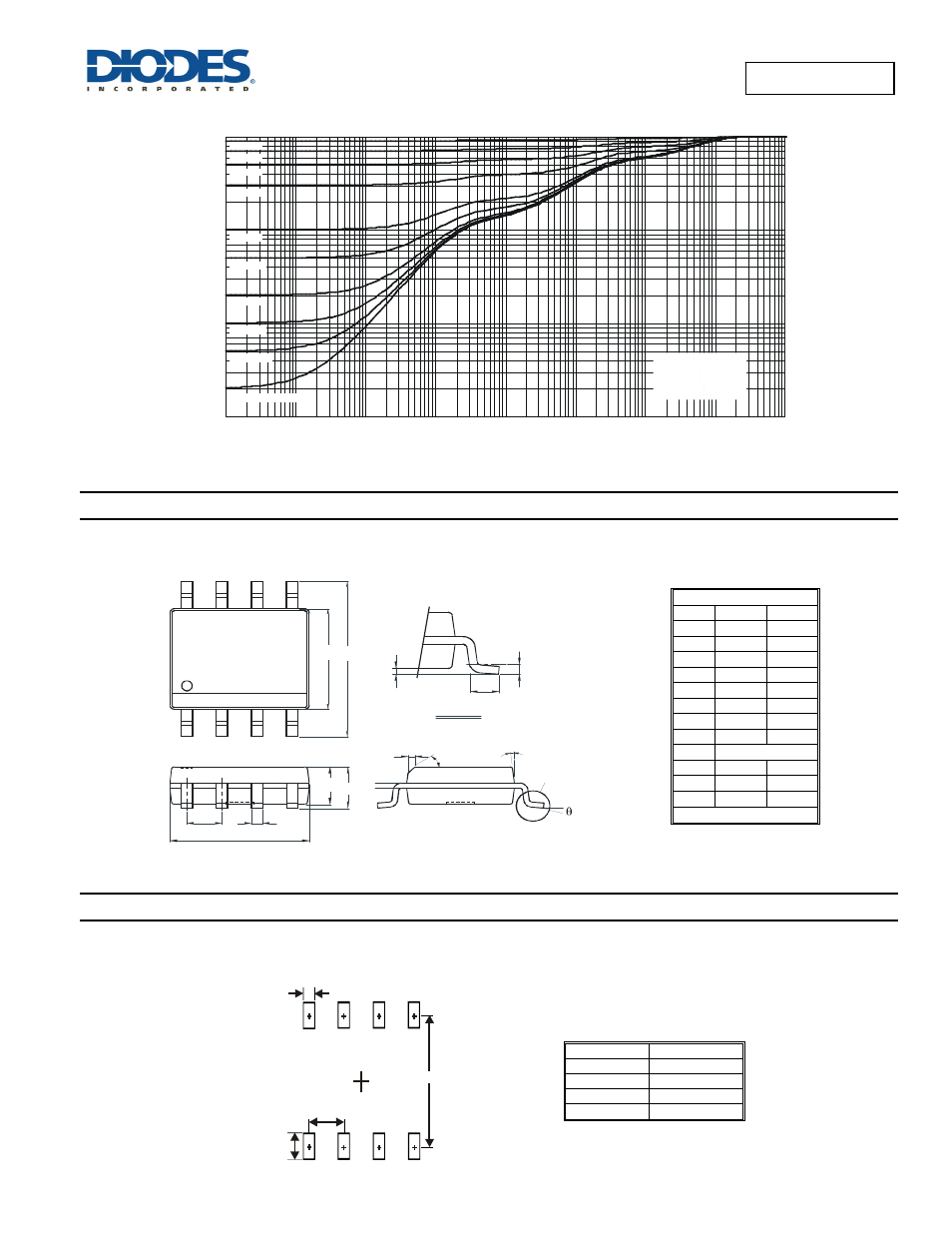
Fig. 12 Transient Thermal Resistance
R
= r * R
θJA(t)
(t)
θ
θ
JA
JA
R
= 85 C/W
Duty Cycle, D = t1/t2
°
0.001
0.01
0.1
1
r(t
),
T
R
ANS
IEN
T
T
H
E
R
MA
L
R
ES
IS
TAN
C
E
D = 0.5
D = 0.7
D = 0.9
D = 0.3
D = 0.1
D = 0.05
D = 0.02
D = 0.01
D = 0.005
D = Single Pulse
Package Outline Dimensions
rsion.
Suggested Pad Layout
e latest version.
SO-8
Dim
Min
Max
A
-
1.75
A1
0.10
0.20
A2
1.30
1.50
A3
0.15
0.25
b
0.3
0.5
D
4.85
4.95
E
5.90
6.10
E1
3.85
3.95
e
1.27 Typ
h
- 0.35
L
0.62 0.82
θ
0
°
8
°
All Dimensions in mm
Dimensions Value (in mm)
X
0.60
Y
1.55
C1
5.4
C2
1.27
Gauge Plane
Seating Plane
Detail ‘A’
Detail ‘A’
E
E1
h
L
D
e
b
A2
A1
A
45
°
7
°~
9
°
A3
0.
25
4
X
C1
C2
Y
- PDS3200 (5 pages)
- PDS340 (5 pages)
- PDS340Q (5 pages)
- PDS360 (5 pages)
- PDS360Q (5 pages)
- PDS4150 (4 pages)
- PDS3100Q (5 pages)
- PDS3100 (5 pages)
- PDS1240CTL (5 pages)
- PDS1045 (5 pages)
- PDS1040L (5 pages)
- PDS1040CTL (5 pages)
- PDS1040 (5 pages)
- PD3S230L (5 pages)
- PD3S230H (3 pages)
- PDS5100Q (5 pages)
- PDS835L (5 pages)
- PDS760 (5 pages)
- PDS560 (5 pages)
- PDS540 (5 pages)
- PDS5100H (5 pages)
- PDS5100 (5 pages)
- PDS4200H (6 pages)
- SBL3060CTP (4 pages)
- SBL30L30CT (3 pages)
- SBL3045CTP (4 pages)
- SBL3040CTP (4 pages)
- SBL2060CTP (4 pages)
- SBL2030CT - SBL2060CT (3 pages)
- SBL2045CTP (4 pages)
- SBL1060CTP (4 pages)
- SBL1040CTP (4 pages)
- SBG3030CT - SBG3045CT (5 pages)
- SB520 - SB560 (3 pages)
- SB370 - SB3100 (3 pages)
- SB320 - SB360 (3 pages)
- SBR10U100CT (5 pages)
- SBR10U150CT (5 pages)
- SBR10A45SP5 (5 pages)
- SBR1060CT (5 pages)
- SBR1045SP5 (5 pages)
- SBR1045SD1 (4 pages)
- SBR1045D1 (5 pages)
- SBR1045CTL (4 pages)
- SBR1040CT (5 pages)