Dmg4822ssd new prod uc t, Maximum ratings, Thermal characteristics – Diodes DMG4822SSD User Manual
Page 2: Electrical characteristics, Dmg4822ssd
DMG4822SSD
Document number: DS35403 Rev. 2 - 2
2 of 7
February 2014
© Diodes Incorporated
DMG4822SSD
NEW PROD
UC
T
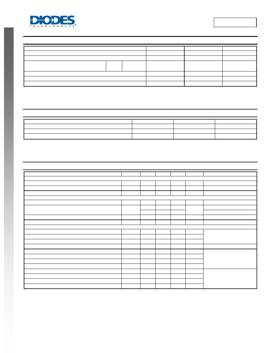
Maximum Ratings
@T
A
= 25°C unless otherwise specified
Characteristic Symbol
Value
Units
Drain-Source Voltage
V
DSS
30 V
Gate-Source Voltage
V
GSS
±25 V
Continuous Drain Current (Note 5) V
GS
= 10V
Steady
State
T
A
= +25°C
T
A
= +85°C
I
D
10
6.6
A
Pulsed Drain Current (Note 6)
I
DM
60 A
Avalanche Current (Note 7 & 8)
I
AR
1.68 A
Repetitive Avalanche Energy L= 0.3mH (Note 7 & 8)
E
AR
12.8 mJ
Thermal Characteristics
@T
A
= 25°C unless otherwise specified
Characteristic Symbol
Value
Units
Total Power Dissipation (Note 5)
P
D
1.42 W
Thermal Resistance, Junction to Ambient (Note 5)
R
θJA
88.4 °C/W
Operating and Storage Temperature Range
T
J,
T
STG
-55 to +150
°C
Electrical Characteristics
@T
A
= 25°C unless otherwise specified
Characteristic
Symbol
Min
Typ
Max
Unit
Test Condition
OFF CHARACTERISTICS (Note 9)
Drain-Source Breakdown Voltage
BV
DSS
30 - - V
V
GS
= 0V, I
D
= 250μA
Zero Gate Voltage Drain Current
I
DSS
- - 1 μA
V
DS
= 30V, V
GS
= 0V
Gate-Source Leakage
I
GSS
- -
±100
nA
V
GS
= ±25V, V
DS
= 0V
ON CHARACTERISTICS (Note 9)
Gate Threshold Voltage
V
GS(th)
1 - 3 V
V
DS
= V
GS
, I
D
= 250μA
Static Drain-Source On-Resistance
R
DS (ON)
- 13.4 20
mΩ
V
GS
= 10V, I
D
= 8.5A
- 19.5 31
V
GS
= 4.5V, I
D
= 6A
Forward Transfer Admittance
|Y
fs
|
- 20 - mS
V
DS
= 5V, I
D
= 8.5A
Diode Forward Voltage
V
SD
- 0.4 1.0 V
V
GS
= 0V, I
S
= 1A
DYNAMIC CHARACTERISTICS (Note 10)
Input Capacitance
C
iss
- 478.9 - pF
V
DS
= 16V, V
GS
= 0V,
f = 1MHz
Output Capacitance
C
oss
- 96.7 - pF
Reverse Transfer Capacitance
C
rss
- 61.4 - pF
Gate resistance
R
g
1.1 Ω
V
DS
= 0V, V
GS
= 0V,f = 1MHz
Total Gate Charge (V
GS
= 4.5V)
Q
g
5 - nC
V
GS
= 10V, V
DS
= 15V,
I
D
=8.5A
Total Gate Charge (V
GS
= 10V)
Q
g
- 10.5 - nC
Gate-Source Charge
Q
gs
- 1.8 - nC
Gate-Drain Charge
Q
gd
- 1.6 - nC
Turn-On Delay Time
t
D(on)
- 2.9 - ns
V
DS
= 15V, V
GS
= 10V,
R
L
= 1.8Ω, R
G
= 3Ω,
Turn-On Rise Time
t
r
- 7.9 - ns
Turn-Off Delay Time
t
D(off)
- 14.6 - ns
Turn-Off Fall Time
t
f
- 3.1 - ns
Notes:
5. Device mounted on FR-4 PCB, with minimum recommended pad layout.
6. Device mounted on minimum recommended pad layout test board, 10μs pulse duty cycle = 1%
7. Repetitive rating, pulse width limited by junction temperature.
8. I
AR
and E
AR
rating are based on low frequency and duty cycles to keep T
j
=+25°C
9. Short duration pulse test used to minimize self-heating effect.
10. Guaranteed by design. Not subject to product testing.