Maximum ratings, Thermal characteristics, Electrical characteristics – Diodes DMG4800LSD User Manual
Page 2: Dmg4800lsd
DMG4800LSD
Document number: DS31858 Rev. 6 - 2
2 of 6
March 2013
© Diodes Incorporated
DMG4800LSD
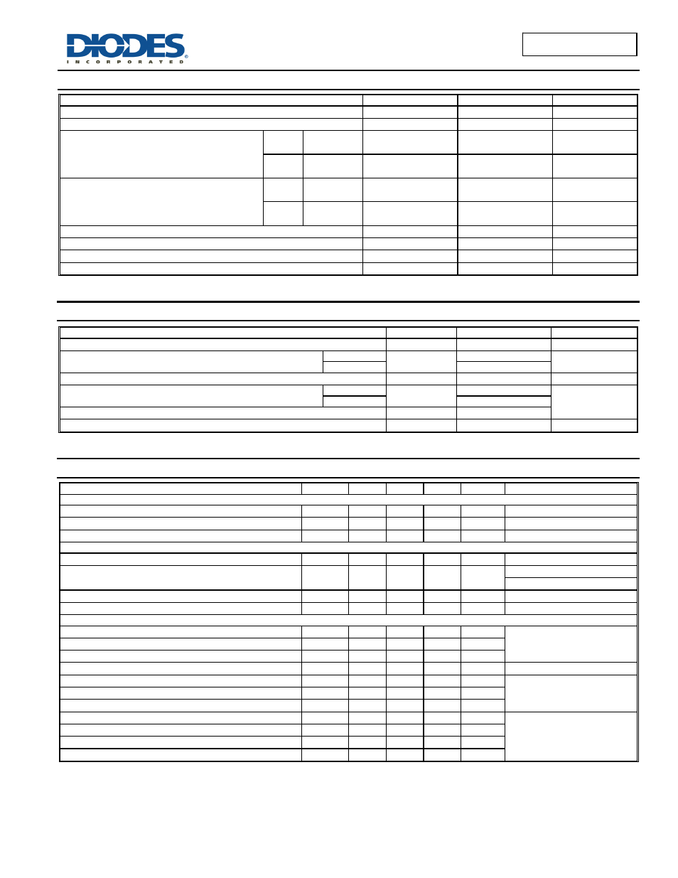
Maximum Ratings
(@T
A
= +25°C, unless otherwise specified.)
Characteristic Symbol
Value
Units
Drain-Source Voltage
V
DSS
30 V
Gate-Source Voltage
V
GSS
±25 V
Continuous Drain Current (Note 6) V
GS
= 10V
Steady
State
T
A
= +25°C
T
A
= +70°C
I
D
7.5
6.0
A
t<10s
T
A
= +25°C
T
A
= +70°C
I
D
9.8
7.7
A
Continuous Drain Current (Note 6) V
GS
= 4.5V
Steady
State
T
A
= +25°C
T
A
= +70°C
I
D
6.4
5.0
A
t<10s
T
A
= +25°C
T
A
= +70°C
I
D
8.4
6.6
A
Maximum Continuous Body Diode Forward Current (Note 6)
I
S
2 A
Pulsed Drain Current (10µs pulse, duty cycle = 1%)
I
DM
42 A
Avalanche Current (Notes 7 & 8) L = 0.1mH
I
AR
17 A
Repetitive Avalanche Energy (Notes 7 & 8) L = 0.1mH
E
AR
14 mJ
Thermal Characteristics
Characteristic Symbol
Value
Units
Total Power Dissipation (Note 5)
P
D
1.17 W
Thermal Resistance, Junction to Ambient (Note 5)
Steady State
R
θJA
107
°C/W
t<10s 61
Total Power Dissipation (Note 6)
P
D
1.5 W
Thermal Resistance, Junction to Ambient (Note 6)
Steady State
R
θJA
83
°C/W
t<10s 49
Thermal Resistance, Junction to Case
R
θJC
14.5
Operating and Storage Temperature Range
T
J,
T
STG
-55 to 150
°C
Electrical Characteristics
(@T
A
= +25°C, unless otherwise specified.)
Characteristic
Symbol
Min
Typ
Max
Unit
Test Condition
OFF CHARACTERISTICS (Note 9)
Drain-Source Breakdown Voltage
BV
DSS
30 - - V
V
GS
= 0V, I
D
= 250μA
Zero Gate Voltage Drain Current T
J
= +25°C
I
DSS
- - 1.0
μA
V
DS
= 30V, V
GS
= 0V
Gate-Source Leakage
I
GSS
- -
±100
nA
V
GS
= ±20V, V
DS
= 0V
ON CHARACTERISTICS (Note 9)
Gate Threshold Voltage
V
GS(th)
0.8 - 1.6 V
V
DS
= V
GS
, I
D
= 250μA
Static Drain-Source On-Resistance
R
DS(on)
-
12
16
16
22
mΩ
V
GS
= 10V, I
D
= 9A
V
GS
= 4.5V, I
D
= 7A
Forward Transfer Admittance
|Y
fs
|
- 8 - S
V
DS
= 10V, I
D
= 9A
Diode Forward Voltage
V
SD
- 0.72
0.94 V
V
GS
= 0V, I
S
= 1A
DYNAMIC CHARACTERISTICS (Note 10)
Input Capacitance
C
iss
- 798 - pF
V
DS
= 10V, V
GS
= 0V,
f = 1.0MHz
Output Capacitance
C
oss
- 128 - pF
Reverse Transfer Capacitance
C
rss
- 122 - pF
Gate Resistance
R
g
- 1.37 - Ω
V
DS
= 0V, V
GS
= 0V, f = 1MHz
Total Gate Charge
Q
g
- 8.56 - nC
V
GS
= 5V, V
DS
= 15V,
I
D
= 9A
Gate-Source Charge
Q
gs
- 1.8 - nC
Gate-Drain Charge
Q
gd
- 2.5 - nC
Turn-On Delay Time
t
D(on)
- 5.03 - ns
V
DD
= 15V, V
GEN
= 10V,
R
L
= 15Ω, R
G
= 6Ω, I
D
= 1A
Turn-On Rise Time
t
r
- 4.50 - ns
Turn-Off Delay Time
t
D(off)
- 26.33 - ns
Turn-Off Fall Time
t
f
- 8.55 - ns
Notes:
5. Device mounted on FR-4 substrate PC board, 2oz copper, with minimum recommended pad layout.
6. Device mounted on FR-4 substrate PC board, 2oz copper, with 1inch square copper plate.
7. I
AR
and E
AR
rating are based on low frequency and duty cycles to keep T
J
= +25°C.
8. Applicable to products manufactured with Data Code “1146” (Nov, 2011) and newer.
9. Short duration pulse test used to minimize self-heating effect.
10. Guaranteed by design. Not subject to product testing.