Dmg4800lfg new prod uc t, Electrical characteristics, Dmg4800lfg – Diodes DMG4800LFG User Manual
Page 2
DMG4800LFG
Document number: DS31785 Rev. 3 - 2
2 of 6
November 2009
© Diodes Incorporated
DMG4800LFG
NEW PROD
UC
T
Electrical Characteristics
@T
A
= 25°C unless otherwise specified
Characteristic
Symbol
Min
Typ
Max
Unit
Test Condition
OFF CHARACTERISTICS (Note 5)
Drain-Source Breakdown Voltage
BV
DSS
30 - - V
V
GS
= 0V, I
D
= 250
μA
Zero Gate Voltage Drain Current TJ = 25°C
I
DSS
- -
1.0
μA
V
DS
= 30V, V
GS
= 0V
Gate-Source Leakage
I
GSS
- -
±100
nA
V
GS
= ±20V, V
DS
= 0V
ON CHARACTERISTICS (Note 5)
Gate Threshold Voltage
V
GS(th)
0.8 - 1.5 V
V
DS
= V
GS
, I
D
= 250
μA
Static Drain-Source On-Resistance
R
DS (ON)
-
11
15
17
24
m
Ω
V
GS
= 10V, I
D
= 9A
V
GS
= 4.5V, I
D
= 7A
Forward Transfer Admittance
|Y
fs
|
- 8 - S
V
DS
= 10V, I
D
= 9A
Diode Forward Voltage
V
SD
- 0.7
1.0 V
V
GS
= 0V, I
S
= 1A
DYNAMIC CHARACTERISTICS (Note 6)
Input Capacitance
C
iss
- 798 - pF
V
DS
= 10V, V
GS
= 0V,
f = 1.0MHz
Output Capacitance
C
oss
- 128 - pF
Reverse Transfer Capacitance
C
rss
- 122 - pF
Gate Resistance
R
g
- 1.37 -
Ω
V
DS
=0V, V
GS
= 0V, f = 1MHz
Total Gate Charge
Q
g
- 9.47 - nC
V
GS
= 5V, V
DS
= 15V,
I
D
= 9A
Gate-Source Charge
Q
gs
- 1.87 - nC
Gate-Drain Charge
Q
gd
- 5.60 - nC
Turn-On Delay Time
t
D(on)
- 5.03 - ns
V
DD
= 15V, V
GEN
= 10V,
R
L
= 15
Ω, R
G
= 6
Ω, I
D
= 1A
Turn-On Rise Time
t
r
- 4.50 - ns
Turn-Off Delay Time
t
D(off)
- 26.33 -
ns
Turn-Off Fall Time
t
f
- 8.55 - ns
Notes:
5. Short duration pulse test used to minimize self-heating effect.
6. Guaranteed by design. Not subject to product testing.
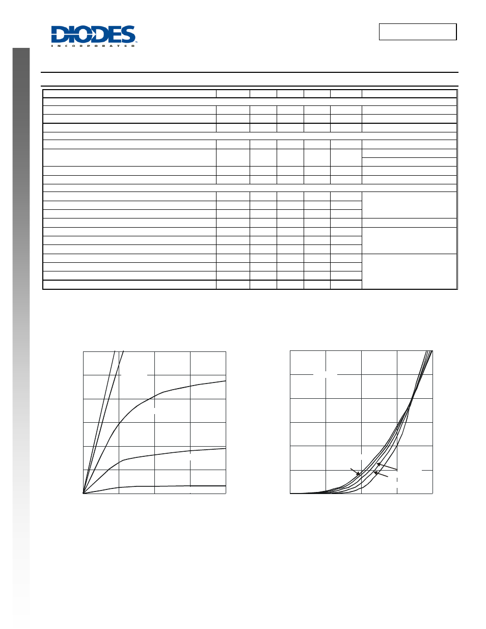
0
0.5
1
1.5
2
0
5
10
15
20
30
I,
D
R
AI
N
C
U
R
R
EN
T
(A
)
D
25
Fig. 1 Typical Output Characteristic
V
, DRAIN-SOURCE VOLTAGE (V)
DS
V
= 2.0V
GS
V
= 3.0V
GS
V
= 4.5V
GS
V
= 10V
GS
V
= 2.5V
GS
I,
D
R
AI
N
C
U
R
R
E
N
T
(A
)
D
0
5
10
15
20
25
30
1
1.5
2
2.5
3
Fig. 2 Typical Transfer Characteristic
V
, GATE-SOURCE VOLTAGE (V)
GS
T = -55°C
A
T = 25°C
A
T = 85°C
A
T = 125°C
A
T = 150°C
A
V
= 5V
DS