Dmg4496sss new prod uc t, Maximum ratings, Thermal characteristics – Diodes DMG4496SSS User Manual
Page 2: Electrical characteristics, Dmg4496sss
DMG4496SSS
Document number: DS32048 Rev. 5 - 2
2 of 6
September 2013
© Diodes Incorporated
DMG4496SSS
NEW PROD
UC
T
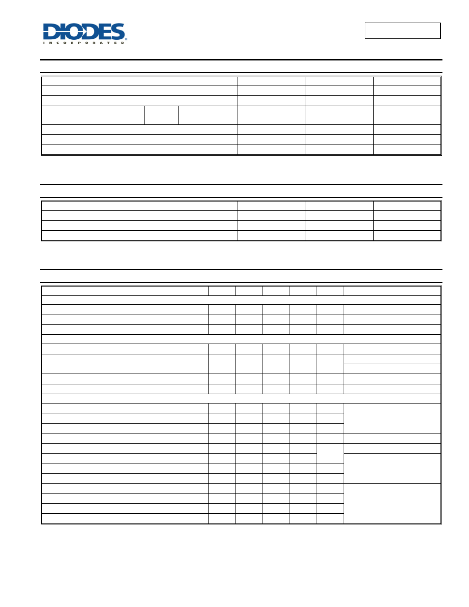
Maximum Ratings
(@T
A
= +25°C, unless otherwise specified.)
Characteristic
Symbol
Value
Unit
Drain-Source Voltage
V
DSS
30 V
Gate-Source Voltage
V
GSS
±25 V
Continuous Drain Current (Note 6)
Steady
State
T
A
= +25°C
T
A
= +85°C
I
D
10
6
A
Pulsed Drain Current (Note 7)
I
DM
60 A
Avalanche Current (Notes 7 & 8)
I
AR
8 A
Repetitive Avalanche Energy (Notes 7 & 8) L = 0.1mH
E
AR
3.2 mJ
Thermal Characteristics
Characteristic Symbol
Value
Unit
Power Dissipation (Note 6)
P
D
1.42 W
Thermal Resistance, Junction to Ambient @T
A
= +25°C (Note 6)
R
θJA
88.49 °C/W
Operating and Storage Temperature Range
T
J
,
T
STG
-55 to +150
°C
Electrical Characteristics
(@T
A
= +25°C, unless otherwise specified.)
Characteristic
Symbol
Min
Typ
Max
Unit
Test Condition
OFF CHARACTERISTICS (Note 9)
Drain-Source Breakdown Voltage
BV
DSS
30
—
— V
V
GS
= 0V, I
D
= 250μA
Zero Gate Voltage Drain Current
I
DSS
— — 1
μA
V
DS
= 30V, V
GS
= 0V
Gate-Source Leakage
I
GSS
— —
±100 nA
V
GS
= ±25V, V
DS
= 0V
ON CHARACTERISTICS (Note 9)
Gate Threshold Voltage
V
GS(th)
0.8 1.2 2.0 V
V
DS
= V
GS
, I
D
= 250μA
Static Drain-Source On-Resistance
R
DS(ON)
—
16
22
21.5
29
mΩ
V
GS
= 10V, I
D
= 10A
V
GS
= 4.5V, I
D
= 7.5A
Forward Transfer Admittance
|Y
fs
|
—
11.7 — S
V
DS
= 5V, I
D
= 10A
Diode Forward Voltage
V
SD
—
0.70 1 V
V
GS
= 0V, I
S
= 1A
DYNAMIC CHARACTERISTICS (Note 10)
Input Capacitance
C
iss
—
493.5
—
pF
V
DS
=15V, V
GS
= 0V,
f = 1.0MHz
Output Capacitance
C
oss
—
94.5
—
pF
Reverse Transfer Capacitance
C
rss
—
50.4
—
pF
Gate Resistance
R
g
—
2.86
—
Ω
V
DS
=0V, V
GS
= 0V, f = 1MHz
Total Gate Charge (V
GS
= 4.5V)
Q
g
—
4.7
—
nC
V
DS
= 15V, V
GS
= 4.5V, ID =10A
Total Gate Charge (V
GS
= 10V)
Q
g
—
10.2
—
V
DS
= 15V, V
GS
= 10V, ID =10A
Gate-Source Charge
Q
gs
—
1.4
—
nC
Gate-Drain Charge
Q
gd
—
1.7
—
nC
Turn-On Delay Time
t
D(on)
—
4.76
—
ns
V
GS
= 10V, V
Ds
= 15V,
R
G
= 6Ω, R
L
= 15Ω,
Turn-On Rise Time
t
r
—
3.64
—
ns
Turn-Off Delay Time
t
D(off)
—
19.5
—
ns
Turn-Off Fall Time
t
f
—
4.9
—
ns
Notes:
6. Device mounted on 1 in.
2
FR-4 board with 2oz. Copper, in a still air environment @ T
A
= +25°C. The value in any given application depends on the
user's specific board design.
7. Repetitive rating, pulse width limited by junction temperature.
8. I
AR
and E
AR
rating are based on low frequency and duty cycles to keep T
J
= 25°C
9. Short duration pulse test used to minimize self-heating effect.
10. Guaranteed by design. Not subject to production testing.