Diodes DEMD48 User Manual
Demd48, Features, Mechanical data
DS31224 Rev. 4 - 2
1 of 4
www.diodes.com
DEMD48
© Diodes Incorporated
DEMD48
DUAL NPN/PNP PRE-BIASED TRANSISTOR
Features
•
Epitaxial Planar Die Construction
•
Surface Mount Package Suited for Automated Assembly
•
Simplifies Circuit Design and Reduces Board Space
•
Lead Free/RoHS Compliant (Note 1)
•
"Green" Device (Note 2)
Mechanical Data
•
Case: SOT-563
•
Case Material: Molded Plastic, “Green” Molding Compound. UL
Flammability Classification Rating 94V-0
•
Moisture Sensitivity: Level 1 per J-STD-020C
•
Terminals: Finish
⎯ Matte Tin Finish annealed over Copper
leadframe. Solderable per MIL-STD-202, Method 208
•
Marking Information: See Page 4
•
Ordering Information: See Page 4
•
Weight: 0.005 grams (approximate)
Reference Device
Type R1(Nom)
R2(Nom)
Q
1
NPN 47k
Ω 47kΩ
Q
2
PNP 2.2
k
Ω 47kΩ
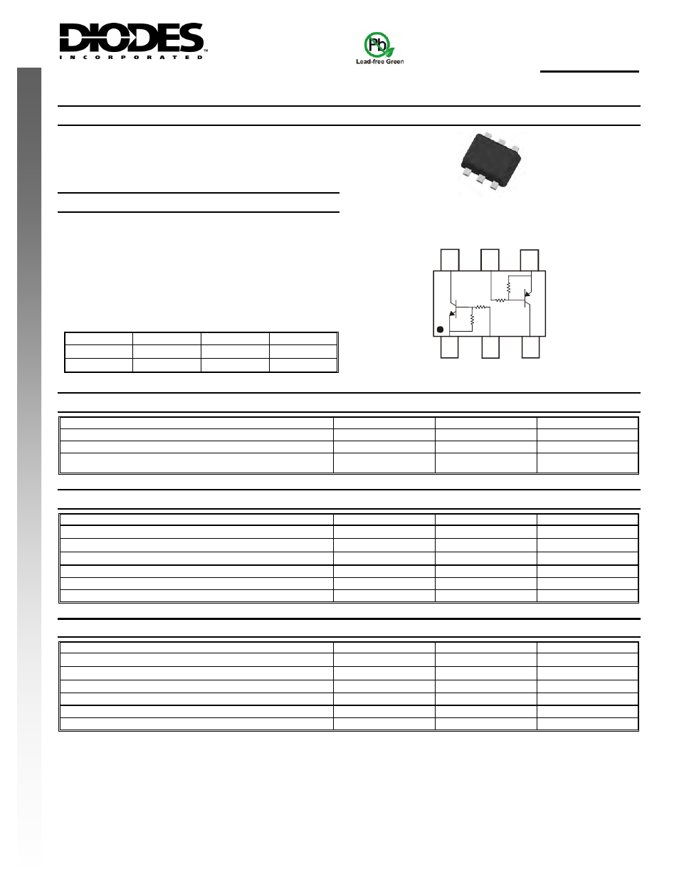
SOT-563
NEW PROD
UC
T
6
Q
1
Q
2
5
4
3
1
2
R
1
R
2
R
1
R
2
47k
47k
2.2k
47k
Maximum Ratings, Total Device
@T
A
= 25°C unless otherwise specified
Characteristic Symbol
Value
Unit
Power Dissipation (Note 3)
P
D
300 mW
Thermal Resistance, Junction to Ambient Air (Note 3)
R
θJA
417 °C/W
Operating and Storage Temperature Range
T
j
, T
STG
-55 to +150
°C
Maximum Ratings, Pre-Biased NPN Transistor, Q
1
@T
A
= 25°C unless otherwise specified
Characteristic Symbol
Value
Unit
Collector-Base Voltage
V
CBO
50 V
Collector-Emitter Voltage
V
CEO
50 V
Emitter-Base Voltage
V
EBO
10 V
Input Voltage
V
IN
-10 to +40
V
Output Current (DC)
I
O
100 mA
Peak Collector Current
I
CM
100 mA
Maximum Ratings, Pre-Biased PNP Transistor, Q
2
@T
A
= 25°C unless otherwise specified
Characteristic Symbol
Value
Unit
Collector-Base Voltage
V
CBO
-50 V
Collector-Emitter Voltage
V
CEO
-50 V
Emitter-Base Voltage
V
EBO
-10 V
Input Voltage
V
IN
-12 to +5
V
Output Current (DC)
I
O
-100 mA
Peak Collector Current
I
CM
-100 mA
Notes:
1. No purposefully added lead.
2. Diodes Inc.'s "Green" policy can be found on our website at http://www.diodes.com/products/lead_free/index.php.
3. Device mounted on FR-4 PCB; pad layout as shown on Diodes Inc. suggested pad layout document AP02001, which can be found on our website at
http://www.diodes.com/datasheets/ap02001.pdf.