Ddtc (r1 r2 series) ca, Marking information, Absolute maximum ratings – Diodes DDTC (R1≠R2 SERIES) CA User Manual
Page 2: Thermal characteristics
DDTC (R1
R2 SERIES) CA
Document number: DS30330 Rev. 11 - 2
2 of 6
November 2013
© Diodes Incorporated
DDTC (R1
R2 SERIES) CA
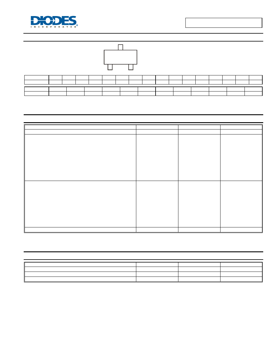
Marking Information
Date Code Key
Year
2002
2003
2004
2005
2006
2007
2008
2009
2010
2011
2012
2013
2014
2015 2016 2017
Code N P R S T U V W X Y Z A B C D E
Month
Jan
Feb
Mar
Apr
May
Jun
Jul
Aug
Sep
Oct
Nov
Dec
Code 1 2 3 4 5 6 7 8 9 O N D
Absolute Maximum Ratings
(@T
A
= +25°C, unless otherwise specified.)
Characteristic Symbol
Value
Unit
Supply Voltage,
V
CC
50 V
Input Voltage,
DDTC113ZCA
DDTC123YCA
DDTC123JCA
DDTC143XCA
DDTC143FCA
DDTC143ZCA
DDTC114YCA
DDTC114WCA
DDTC124XCA
DDTC144VCA
DDTC144WCA
V
IN
-5 to +10
-5 to +12
-5 to +12
-7 to +20
-6 to +30
-5 to +30
-6 to +40
-10 to +30
-10 to +40
-15 to +40
-10 to +40
V
Output Current
DDTC113ZCA
DDTC123YCA
DDTC123JCA
DDTC143XCA
DDTC143FCA
DDTC143ZCA
DDTC114YCA
DDTC114WCA
DDTC124XCA
DDTC144VCA
DDTC144WCA
I
O
100
100
100
100
100
100
70
100
50
30
30
mA
Output Current All
I
C(MAX)
100 mA
Thermal Characteristics
(@T
A
= +25°C, unless otherwise specified.)
Characteristic
Symbol
Value
Unit
Power Dissipation (Note 6)
P
D
200
mW
Thermal Resistance, Junction to Ambient Air (Note 6)
R
θJA
625
C/W
Operating and Storage Temperature Range
T
J
, T
STG
-55 to +150
C
Notes:
6. Mounted on FR4 PC Board with minimum recommended pad layout
Nxx = Product Type Marking Code (See Table Above)
YM = Date Code Marking
Y = Year (ex: T = 2006)
M = Month (ex: 9 = September)
Nxx
YM