Diodes DDTA (R1 = R2 SERIES) CA User Manual
Ddta (r1 = r2 series) ca, Features, Mechanical data
DDTA(R1 = R2 SERIES) CA
Document number: DS30333 Rev. 9 - 2
1 of 5
November 2013
© Diodes Incorporated
DDTA (R1 = R2 SERIES) CA
PNP PRE-BIASED SMALL SIGNAL SURFACE MOUNT TRANSISTOR
Features
Epitaxial Planar Die Construction
Complementary NPN Types Available (DDTC)
Built-In Biasing Resistors, R1
R2
Totally Lead-Free & Fully RoHS compliant (Notes 1 & 2)
Halogen and Antimony Free "Green" Device (Note 3)
Qualified to AEC-Q101 Standards for High Reliability
PPAP Capable (Note 4)
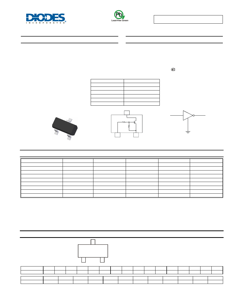
Mechanical Data
Case:
SOT23
Case Material: Molded Plastic, “Green” Molding Compound
UL Flammability Classification Rating 94V-0
Moisture Sensitivity: Level 1 per J-STD-020
Terminals: Finish – Matte Tin Plated Leads, Solderable per
MIL-STD-202, Method 208
Weight: 0.008 grams (approximate)
Part Number
R1, R2 (NOM)
DDTA123ECA 2.2KΩ
DDTA143ECA 4.7KΩ
DDTA114ECA 10KΩ
DDTA124ECA 22KΩ
DDTA144ECA 47KΩ
DDTA115ECA 100KΩ
Ordering Information
(Notes 3 & 4)
Product
Compliance
Marking
Reel size (inches)
Tape width (mm)
Quantity per reel
DDTA123ECA-7-F AEC-Q101
P04
7
8
3,000
DDTA143ECA-7-F AEC-Q101
P08
7
8
3,000
DDTA114ECA-7-F AEC-Q101
P13
7
8
3,000
DDTA114ECAQ-7-F Automotive
P13
7
8
3,000
DDTA114ECAQ-13-F Automotive
P13
13
8
10,000
DDTA124ECA-7-F AEC-Q101
P17
7
8
3,000
DDTA144ECA-7-F AEC-Q101
P20
7
8
3,000
DDTA144ECAQ-13-F Automotive
P20
13
8
10,000
DDTA115ECA-7-F AEC-Q101
P24
7
8
3,000
Notes:
1. No purposely added lead. Fully EU Directive 2002/95/EC (RoHS) & 2011/65/EU (RoHS 2) compliant.
2. S more information about Diodes Incorporated’s definitions of Halogen- and Antimony-free, "Green"
and Lead-free.
3. Halogen- and Antimony-free "Green” products are defined as those which contain <900ppm bromine, <900ppm chlorine (<1500ppm total Br + Cl) and
<1000ppm antimony compounds.
4. Automotive products are AEC-Q101 qualified and are PPAP capable. Automotive, AEC-Q101 and standard products are electrically and thermally the
same, except where specified. For more information, please refer to
5. For packaging details, go to our website at
Marking Information
Date Code Key
Year
2002
2003
2004
2005
2006 2007
2008
2009
2010
2011 2012
2013
2014
2015
2016
2017
Code N P R S T U V W X Y Z A B C D E
Month
Jan
Feb
Mar
Apr
May
Jun
Jul
Aug
Sep
Oct
Nov
Dec
Code 1 2 3 4 5 6 7 8 9 O N D
Device Schematic
Top View
SOT23
XXX = Product Type Marking Code, See Ordering Information
YM = Date Code Marking
Y = Year (ex: X = 2010)
M = Month (ex: 9 = September)
1
3
2
GND (0)
C
B
IN
OUT
E
Equivalent Inverter Circuit
R1
OUT
B
C
E
R2
3
2
1
IN
GND(+)
XXX
YM