Electrical characteristics, Drdc3105, A product line of diodes incorporated – Diodes DRDC3105 User Manual
Page 3
DRDC3105
Document number: DS35213
Rev. 4 - 2
3 of 9
March 2013
© Diodes Incorporated
A Product Line of
Diodes Incorporated
DRDC3105
Electrical Characteristics
(@T
A
= +25°C, unless otherwise specified.)
Characteristic Symbol
Min
Typ
Max
Unit
Test
Condition
OFF CHARACTERISTICS
Output Zener Breakdown Voltage
BV
(out)
BV
(−out)
6.2
-
6.6
0.67
7.0
-
V
@ I
T
= 10 mA Pulse
Output Leakage Current @ 0 Input Voltage
I
OO
—
—
—
—
0.1
30
µA
V
O
= 5.5 V, T
A
= +25°C
V
O
= 5.5 V, T
A
= +85°C
“ON” state input voltage (Note 13)
V
in(on)
—
0.99 1.5 V I
O
=100 mA, V
O
= 150mV
“OFF” State Input Voltage (Note 14)
V
in(off)
400 540
—
mV
I
O
=100 µA, V
O
= 4.9V
ON CHARACTERISTICS
Input Bias Current (H
FE
Limited)
I
in
—
0.7 1.6 mA
I
O
= 250 mA, V
O
= 0.25V
Output Saturation Voltage
V
O(sat)
—
125 160 mV
I
O
= 250 mA, I
in
= 1.5 mA
Output Sink Current – Continuous
I
O(on)
250 430
—
mA
V
CE
= 0.25 V, I
in
= 1.5 mA
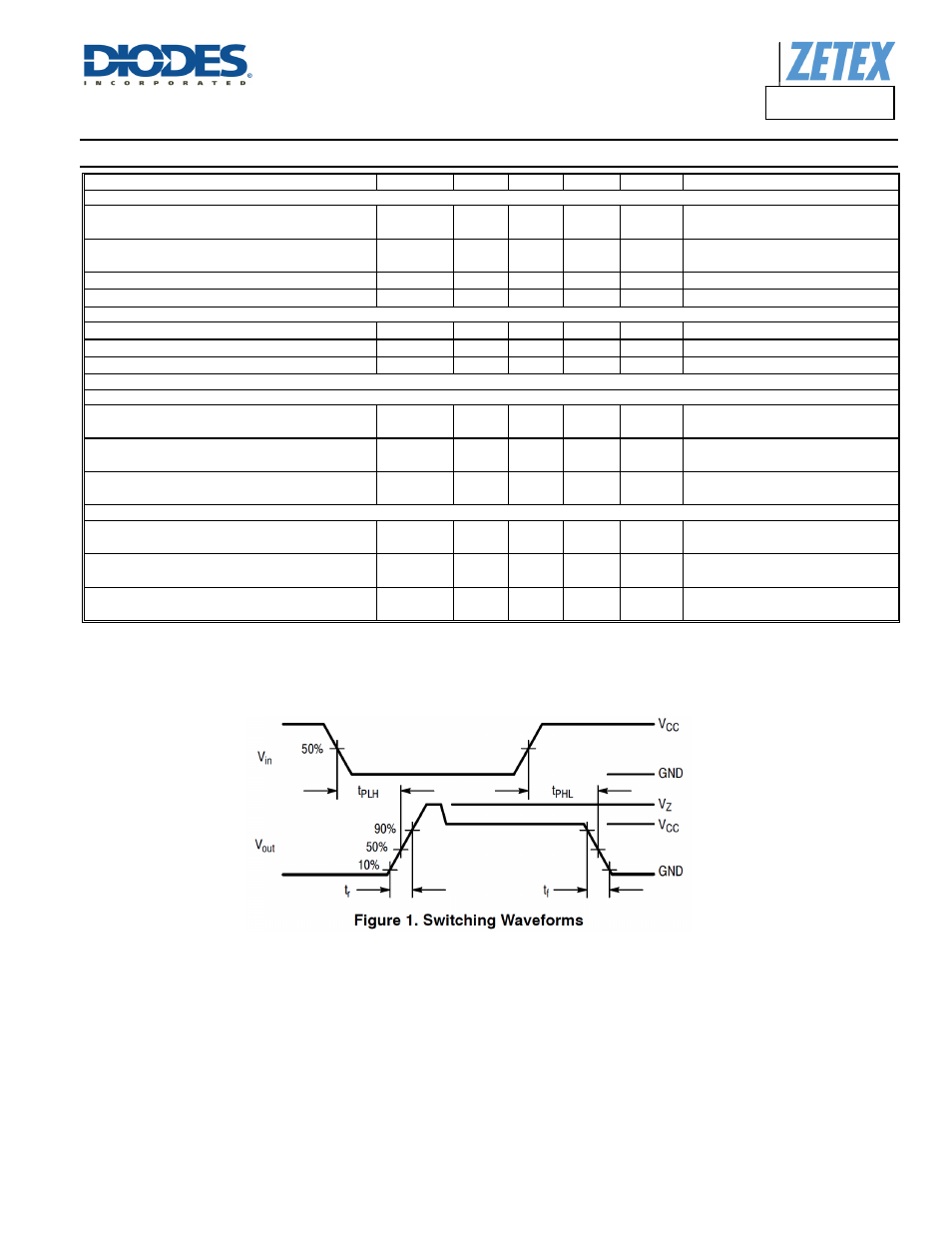
SWITCHING CHARACTERISTICS (Refer to Figure 1)
Propagation Delay Times:
High to Low Propagation Delay; (5.0V 74HC04)
Low to High Propagation Delay; (5.0V 74HC04)
t
PHL
t
PLH
—
20.4
1.43
—
ns
µs
—
High to Low Propagation Delay; 13 (3.0V 74HC04)
Low to High Propagation Delay; 13 (3.0V 74HC04)
t
PHL
t
PLH
—
32.2
760
—
ns
ns
—
High to Low Propagation Delay; 14 (5.0V 74LS04)
Low to High Propagation Delay; 14 (5.0V 74LS04)
t
PHL
t
PLH
—
25.3
2.57
—
ns
µs
—
Transition Times:
Fall Time; (5.0V 74HC04)
Rise Time; (5.0V 74HC04)
t
f
t
r
—
12.5
411
—
ns
ns
—
Fall Time; 13 (3.0V 74HC04)
Rise Time; 13 (3.0V 74HC04)
t
f
t
r
—
21.1
220
—
ns
ns
—
Fall Time; 14 (5.0V 74LS04)
Rise Time; 14 (5.0V 74LS04)
t
f
t
r
—
15.1
849
—
ns
ns
—
Notes:
13. The device is guaranteed to be in “ON” state with V
IN(ON)
above 1.5V
14. The device is guaranteed to be in “OFF” state with V
IN(OFF)
below 400mV