Drdc3105, Internal device schematic, Maximum ratings – Diodes DRDC3105 User Manual
Page 2: Thermal characteristics
DRDC3105
Document number: DS35213
Rev. 4 - 2
2 of 9
March 2013
© Diodes Incorporated
A Product Line of
Diodes Incorporated
DRDC3105
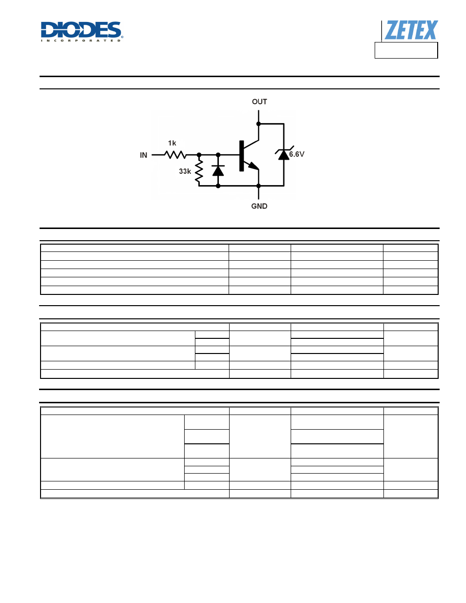
Internal Device Schematic
Maximum Ratings
(@T
A
= +25°C, unless otherwise specified.)
Characteristic Symbol
Limit
Unit
Supply Voltage
V
CC
6.0 V
Input Voltage (Forward)
V
IN(FWD)
6.0 V
Input Voltage (Reverse)
V
IN(REV)
-0.5 V
Output Sink Continuous Current
I
O
500 mA
Repetitive Pulse Zener Energy Limit (Duty Cycle 0.01%)
E
zpk
50 mJ
Thermal Characteristics for DRDC3105F (SOT23)
(@T
A
= +25°C, unless otherwise specified.)
Characteristic Symbol
Value
Unit
Power Dissipation
(Note 5)
P
D
310
mW
(Note 6)
350
Thermal Resistance, Junction to Ambient
(Note 5)
R
θJA
403
°C/W
(Note 6)
357
Thermal Resistance, Junction to Leads
(Note 11)
R
θJL
350 °C/W
Operating and Storage Temperature Range
T
J,
T
STG
-55 to +150
°C
Thermal Characteristics
for DRDC3105E6 (SOT26)
(@T
A
= +25°C, unless otherwise specified.)
Characteristic Symbol
Value
Unit
Power Dissipation
Linear Derating Factor
(Note 7 & 9)
P
D
0.9
7.2
W
mW/°C
(Note 7 & 10)
1.1
8.8
(Note 8 & 10)
1.7
13.6
Thermal Resistance, Junction to Ambient
(Note 7 & 9)
R
θJA
139
°C/W
(Note 7 & 10)
113
(Note 8 & 10)
73
Thermal Resistance, Junction to Leads
(Note 11)
R
θJL
100 °C/W
Operating and Storage Temperature Range
T
J
, T
STG
-55 to +150
°C
Notes:
5. For a device mounted on minimum recommended pad layout 1oz weight copper that is on a single-sided FR4 PCB; device is measured under still air
conditions whilst operating in a steady-state.
6. Same as Note 5, except the device is mounted on 15mm X 15mm 1oz copper.
7. Same as Note 5, except the device is mounted on 25mm X 25mm 1oz copper.
8. Same as Note 7, except the device is measured at < 5sec
9. For a device with one active die.
10. For a device with two die running at equal power.
11. Thermal resistance from junction to solder-point (at the end of the “OUT” lead).