Electrical characteristics, Dxt696bk – Diodes DXT696BK User Manual
Page 4
DXT696BK
Document number: DS36574 Rev. 1 - 2
4 of 7
December 2013
© Diodes Incorporated
DXT696BK
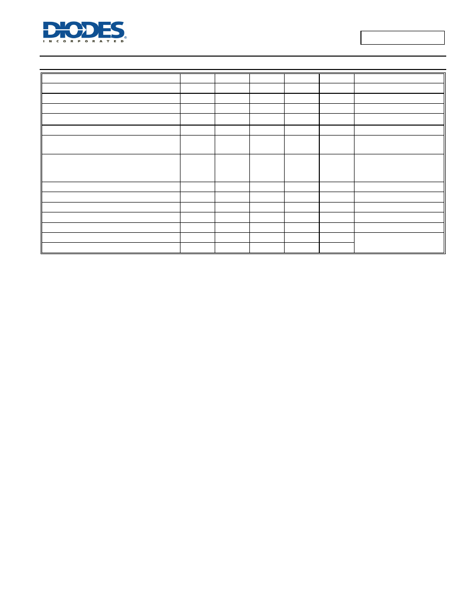
Electrical Characteristics
(@T
A
= +25°C, unless otherwise specified.)
Characteristic Symbol
Min
Typ
Max
Unit
Test
Condition
Collector-Base Breakdown Voltage
BV
CBO
180 — — V
I
C
= 100µA
Collector-Emitter Breakdown Voltage (Note 11)
BV
CEO
180 — — V
I
C
= 1mA
Emitter-Base Breakdown Voltage
BV
EBO
7 — — V
I
E
= 100µA
Collector-Base Cutoff Current
I
CBO
—
—
100 nA
V
CB
= 140V
Emitter Cutoff Current
I
EBO
— — 100 nA
V
EB
= 5V
DC Current Gain (Note 11)
h
FE
500
150
—
—
—
—
I
C
= 100mA, V
CE
= 5V
I
C
= 200mA, V
CE
= 5V
Collector-Emitter Saturation Voltage (Note 11)
V
CE(sat)
—
—
—
—
—
—
200
200
250
mV
I
C
= 50mA, I
B
= 0.5mA
Ic = 100mA, I
B
= 2.0mA
I
C
= 200mA, I
B
= 5.0mA
Base-Emitter Saturation Voltage (Note 11)
V
BE(sat)
— — 900
mV
I
C
= 200mA, I
B
= 5mA
Base-Emitter Turn-On Voltage (Note 11)
V
BE(on)
— — 900
mV
I
C
= 200mA, V
CE
= 5V
Input Capacitance
C
ibo
— 200 — pF
V
EB
= 0.5V, f = 1MHz
Output Capacitance
C
obo
— 6 — pF
V
CE
= 10V, f = 1MHz
Current Gain-Bandwidth Product
f
T
70 — — MHz
V
CE
= 5V, I
C
= 50mA, f=50MHz
Turn-On Time
t
on
— 80 — ns
V
CC
= 50V, I
C
= 100mA
I
B1
= -I
B2
= 10mA
Turn-Off Time
t
off
— 4,400 — ns
Note:
11. Measured under pulsed conditions. Pulse width ≤ 300 µs. Duty cycle ≤ 2%.