Fzt653, Package outline dimensions, Suggested pad layout – Diodes FZT653 User Manual
Page 6
FZT653
Document Number DS33150 Rev. 4 - 2
6 of 7
November 2013
© Diodes Incorporated
A Product Line of
Diodes Incorporated
FZT653
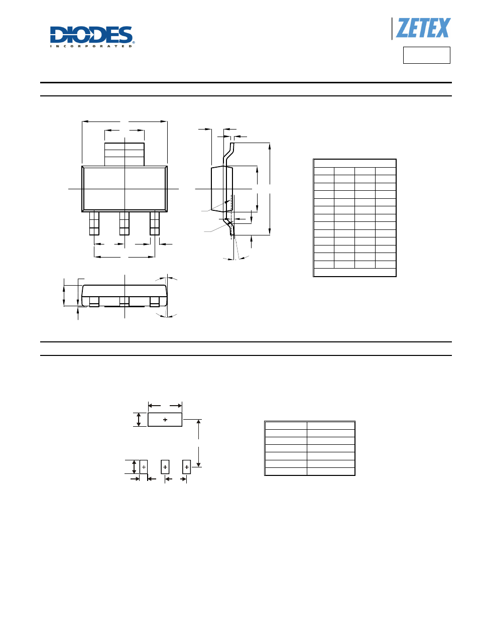
Package Outline Dimensions
rsion.
Suggested Pad Layout
e latest version.
Note: For high voltage applications, the appropriate industry sector guidelines should be considered with regards to creepage and clearance distances between device
Terminals and PCB tracking.
SOT223
Dim Min Max Typ
A 1.55
1.65
1.60
A1 0.010 0.15 0.05
b1 2.90 3.10 3.00
b2 0.60 0.80 0.70
C 0.20
0.30
0.25
D 6.45
6.55
6.50
E 3.45
3.55
3.50
E1 6.90 7.10 7.00
e — —
4.60
e1 — — 2.30
L 0.85
1.05
0.95
Q 0.84
0.94
0.89
All Dimensions in mm
Dimensions Value (in mm)
X1
3.3
X2
1.2
Y1
1.6
Y2
1.6
C1
6.4
C2
2.3
X2
C1
C2
X1
Y2
Y1
A1
A
7°
7°
D
b
e
e1
b1
C
E1
L
0°-
10
°
Q
E
0.25
Seating
Plane
Gauge
Plane
- PDS3200 (5 pages)
- PDS340 (5 pages)
- PDS340Q (5 pages)
- PDS360 (5 pages)
- PDS360Q (5 pages)
- PDS4150 (4 pages)
- PDS3100Q (5 pages)
- PDS3100 (5 pages)
- PDS1240CTL (5 pages)
- PDS1045 (5 pages)
- PDS1040L (5 pages)
- PDS1040CTL (5 pages)
- PDS1040 (5 pages)
- PD3S230L (5 pages)
- PD3S230H (3 pages)
- PDS5100Q (5 pages)
- PDS835L (5 pages)
- PDS760 (5 pages)
- PDS560 (5 pages)
- PDS540 (5 pages)
- PDS5100H (5 pages)
- PDS5100 (5 pages)
- PDS4200H (6 pages)
- SBL3060CTP (4 pages)
- SBL30L30CT (3 pages)
- SBL3045CTP (4 pages)
- SBL3040CTP (4 pages)
- SBL2060CTP (4 pages)
- SBL2030CT - SBL2060CT (3 pages)
- SBL2045CTP (4 pages)
- SBL1060CTP (4 pages)
- SBL1040CTP (4 pages)
- SBG3030CT - SBG3045CT (5 pages)
- SB520 - SB560 (3 pages)
- SB370 - SB3100 (3 pages)
- SB320 - SB360 (3 pages)
- SBR10U100CT (5 pages)
- SBR10U150CT (5 pages)
- SBR10A45SP5 (5 pages)
- SBR1060CT (5 pages)
- SBR1045SP5 (5 pages)
- SBR1045SD1 (4 pages)
- SBR1045D1 (5 pages)
- SBR1045CTL (4 pages)
- SBR1040CT (5 pages)