Fcx493, Maximum ratings, Thermal characteristics – Diodes FCX493 User Manual
Page 2: Thermal characteristics and derating information, Safe operating area, Derating curve, Transient thermal impedance, Pulse power dissipation
FCX493
Da
tasheet Number: DS33056 Rev. 6 - 2
2 of 6
October 2012
© Diodes Incorporated
FCX493
A Product Line of
Diodes Incorporated
Maximum Ratings
(@T
A
= +25°C, unless otherwise specified.)
Characteristic Symbol
Value
Unit
Collector-Base Voltage
V
CBO
120 V
Collector-Emitter Voltage
V
CEO
100 V
Emitter-Base Voltage
V
EBO
7 V
Continuous Collector Current
I
C
1 A
Peak Pulse Current
I
CM
2 A
Continuous Base Current
I
B
200 mA
Thermal Characteristics
(@T
A
= +25°C, unless otherwise specified.)
Characteristic Symbol
Value
Unit
Collector Power Dissipation (Note 5)
P
D
1 W
Thermal Resistance, Junction to Ambient Air (Note 5)
R
θJA
125
°C/W
Thermal Resistance, Junction to Leads (Note 6)
R
θJL
10.01
°C/W
Operating and Storage Temperature Range
T
J,
T
STG
-65 to +150
°C
Notes:
5. For the device mounted on 15mm x 15mm x 1.6mm FR4 PCB with high coverage of single sided 1oz copper, in still air conditions.
6. Thermal resistance from junction to solder-point (on the exposed collector pad).
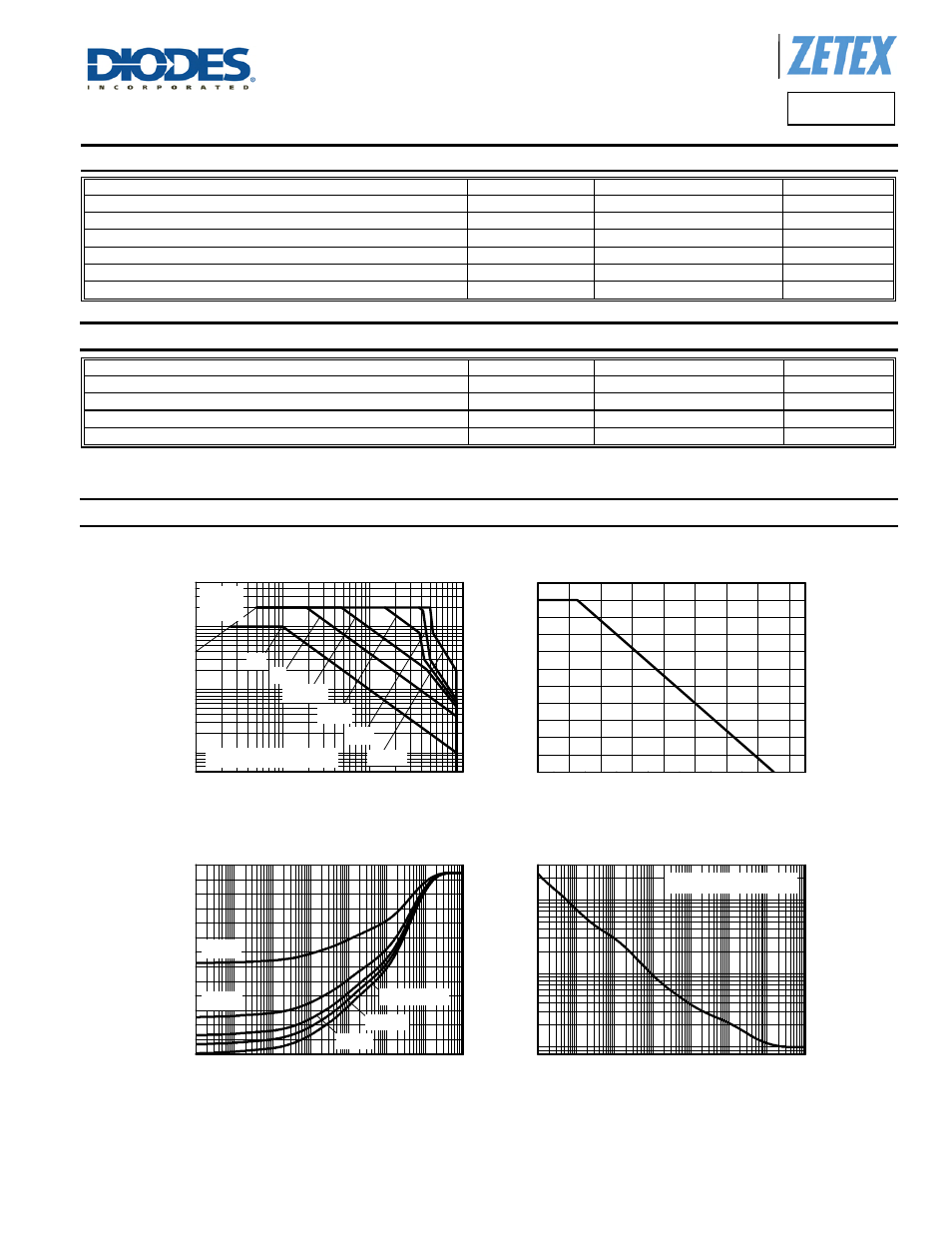
Thermal Characteristics and Derating Information
100m
1
10
100
10m
100m
1
Single Pulse. T
amb
=25°C
V
CE(sat)
Limited
100µs
1ms
10ms
100ms
1s
DC
Safe Operating Area
I
C
C
o
lle
c
to
r C
u
rr
e
n
t (
A
)
V
CE
Collector-Emitter Voltage (V)
0
20
40
60
80
100 120 140 160
0.0
0.2
0.4
0.6
0.8
1.0
Derating Curve
Temperature (°C)
Ma
x
Pow
e
r D
is
s
ip
atio
n
(
W
)
100µ
1m
10m 100m
1
10
100
1k
0
20
40
60
80
100
120
Transient Thermal Impedance
D=0.5
D=0.2
D=0.1
Single Pulse
D=0.05
T
h
er
m
a
l Resi
s
tance
(°
C/
W)
Pulse Width (s)
100µ
1m
10m 100m
1
10
100
1k
1
10
100
Single Pulse. T
amb
=25°C
Pulse Power Dissipation
Pulse Width (s)
M
a
x P
o
wer
Di
ssi
p
a
ti
on
(W
)