Fcx491, Electrical characteristics, A product line of diodes incorporated – Diodes FCX491 User Manual
Page 4
FCX491
Document number: DS33054 Rev. 5 - 2
4 of 7
April 2014
© Diodes Incorporated
FCX491
A Product Line of
Diodes Incorporated
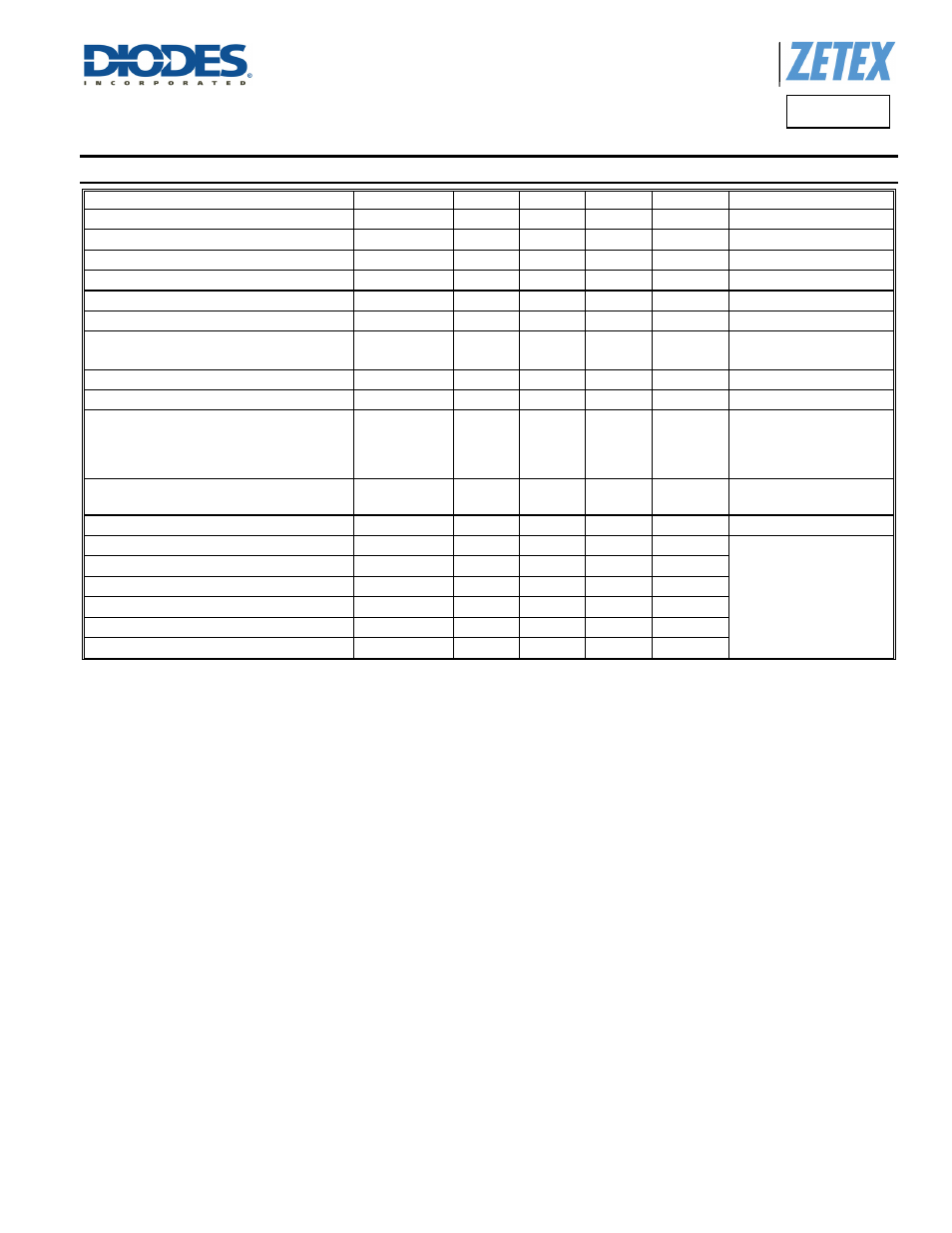
Electrical Characteristics
(@T
A
= +25°C, unless otherwise specified.)
Characteristic Symbol
Min
Typ
Max
Unit
Test
Condition
Collector-Base Breakdown Voltage
BV
CBO
80 — — V
I
C
= 100µA
Collector-Emitter Breakdown Voltage (Note 11)
BV
CEO
60 — — V
I
C
= 10mA
Emitter-Base Breakdown Voltage
BV
EBO
7 8.1 — V
I
E
= 100µA
Collector-Base Cutoff Current
I
CBO
— <1 100 nA
V
CB
= 60V
Collector Cutoff Current
I
CES
— <1 100 nA
V
CES
= 60V
Emitter Cutoff Current
I
EBO
— <1 100 nA
V
EB
= 5.6V
Collector-Emitter Saturation Voltage (Note 11)
V
CE(sat)
—
—
100
160
250
500
mV
I
C
= 500mA, I
B
= 50mA
I
C
= 1A, I
B
= 100mA
Base-Emitter Saturation Voltage (Note 11)
V
BE(sat)
— 965
1100 mV
I
C
= 1A, I
B
= 100mA
Base-Emitter Turn-On Voltage (Note 11)
V
BE(on)
— 830
1000 mV
I
C
= 1A, V
CE
= 5V
DC Current Gain (Note 11)
h
FE
100
100
80
30
140
150
120
40
300 —
I
C
= 1mA, V
CE
= 5V
I
C
= 500mA, V
CE
= 5V
I
C
= 1A, V
CE
= 50V
I
C
= 2A, V
CE
= 5V
Transitional Frequency
f
T
150 — — MHz
I
C
= 50mA, V
CE
= 10V
f=100MHz
Output capacitance
C
obo
— — 10 pF
V
CB
= 10V, f=1MHz
Turn-On Time
t
on
—
49 —
ns
V
CC
= 10V,
I
CC
= 0.5A
I
B1
= - I
B2
= 25mA
Delay Time
t
d
—
18 —
ns
Rise Time
t
r
—
31 —
ns
Turn-Off Time
t
off
—
476 —
ns
Storage Time
t
s
—
414 —
ns
Fall Time
t
f
—
62 —
ns
Note:
11. Measured under pulsed conditions. Pulse width
≤
300
µs. Duty cycle ≤ 2%