Electrical characteristics, Dxt5616u, A product line of diodes incorporated – Diodes DXT5616U User Manual
Page 4
DXT5616U
Datasheet Number: DS37030 Rev. 1 – 2
4 of 7
March 2014
© Diodes Incorporated
DXT5616U
A Product Line of
Diodes Incorporated
Electrical Characteristics
(@T
A
= +25°C, unless otherwise specified.)
Characteristic Symbol
Min
Typ
Max
Unit
Test
Condition
Collector-Base
Breakdown Voltage
BV
CBO
100 — — V
I
C
= 100µA
Collector-Emitter
Breakdown Voltage (Note 6)
BV
CEO
80 — — V
I
C
= 10mA
Emitter-Base Breakdown Voltage
BV
EBO
7 — — V
I
E
= 100µA
Collector Cut-off Current
I
CBO
— —
0.1
20
µ
A
V
CB
= 80V
V
CB
= 80V, T
A
= +150°C
Emitter Cut-off Current
I
EBO
— — 20 nA
V
EB
= 6V
Static Forward Current Transfer Ratio (Note 6)
h
FE
25
100
25
—
—
—
—
250
—
I
C
= 5mA, V
CE
= 2V
I
C
= 150mA, V
CE
= 2V
I
C
= 500mA, V
CE
= 2V
Collector-Emitter Saturation Voltage (Note 6)
V
CE(sat)
— — 0.5 V
I
C
= 500mA, I
B
= 50mA
Base-Emitter Turn-On Voltage (Note 6)
V
BE(on)
— — 1.0 V
I
C
= 500mA, V
CE
= 2V
Transition Frequency
f
T
150
—
—
MHz
I
C
= 50mA, V
CE
= 10V
f = 100MHz
Output Capacitance
C
obo
— — 25 pF
V
CB
= 10V, f = 1MHz
Delay Time
t
d
— 21 —
ns
I
C
= 400mA, V
CC
= 40V,
I
B1
= 20mA, I
B2
= -20mA
Rise Time
t
r
— 33 —
Storage Time with Resistive Load
t
s
— 708 —
Fall Time with Resistive Load
t
f
— 95 —
Notes:
6. Measured under pulsed conditions. Pulse width ≤ 300µs. Duty cycle ≤ 2%.
0
0.2
0.4
0.6
0.8
0
1
2
3
4
5
V , COLLECTOR-EMITTER VOLTAGE (V)
CE
I,
C
O
LL
E
C
T
O
R
C
U
R
R
E
N
T
(A
)
C
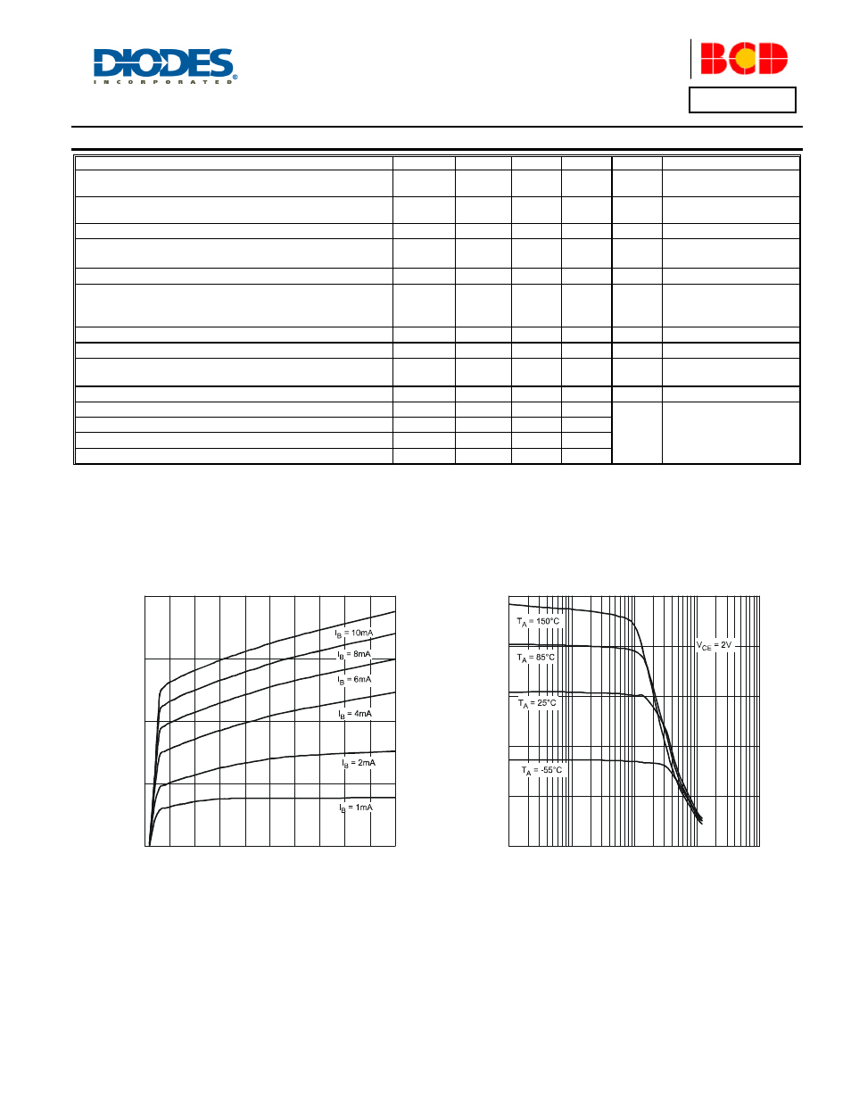
Fig. 1 Typical Collector Current
vs. Collector-Emitter Voltage
h
, DC CU
RR
ENT
GAIN
FE
Fig. 2 Typical DC Current Gain vs. Collector Current
0
50
100
150
200
250
0.001
0.01
0.1
1
10
I , COLLECTOR CURRENT (A)
C