Maximum ratings, Thermal characteristics, Electrical characteristics – Diodes FMMT549A User Manual
Page 2: A product line of diodes incorporated
FMMT549 / FMMT549A
Document Number: DS33098 Rev. 4 - 2
2 of 5
September 2011
© Diodes Incorporated
A Product Line of
Diodes Incorporated
FMMT549 / FMMT549A
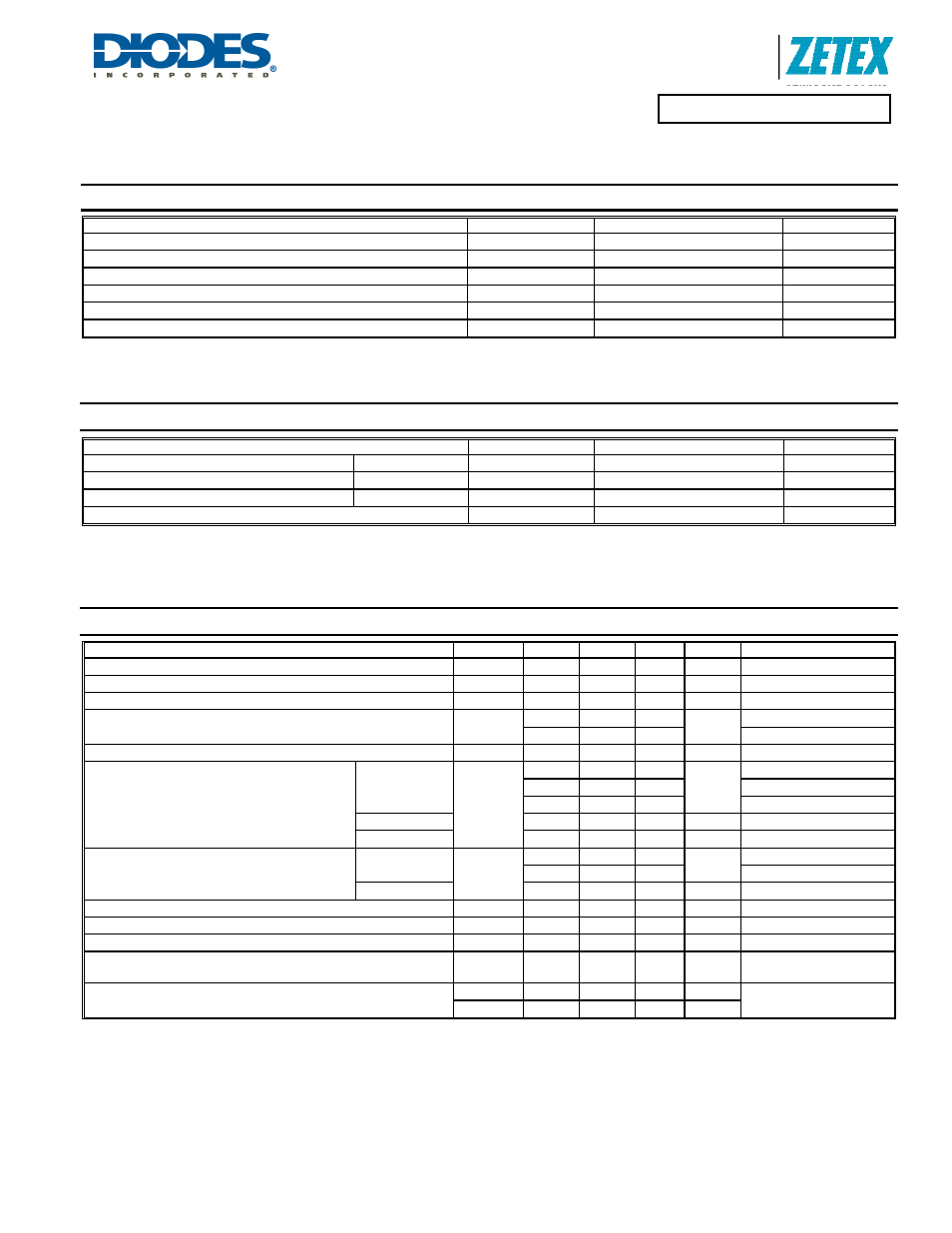
Maximum Ratings
@T
A
= 25°C unless otherwise specified
Characteristic Symbol
Value
Unit
Collector-Base Voltage
V
CBO
-35 V
Collector-Emitter Voltage
V
CEO
-30 V
Emitter-Base Voltage
V
EBO
-5 V
Continuous Collector Current
I
C
-1 A
Peak Pulse Current
I
CM
-2 A
Base Current
I
B
-200 mA
Thermal Characteristics
@T
A
= 25°C unless otherwise specified
Characteristic Symbol
Value
Unit
Power Dissipation
(Note 4)
P
D
500 mW
Thermal Resistance, Junction to Ambient
(Note 4)
R
θJA
250
°C/W
Thermal Resistance, Junction to Lead
(Note 5)
R
θJL
197
°C/W
Operating and Storage Temperature Range
T
J,
T
STG
-55 to +150
°C
Electrical Characteristics
@T
A
= 25°C unless otherwise specified
Characteristic Symbol
Min
Typ
Max
Unit
Test
Condition
Collector-Base Breakdown Voltage
BV
CBO
-35 - - V
I
C
= -100µA
Collector-Emitter Breakdown Voltage (Note 6)
BV
CEO
-30 - - V
I
C
= -10mA
Emitter-Base Breakdown Voltage
BV
EBO
-5 - - V
I
E
= -100µA
Collector Cutoff Current
I
CBO
- -
-0.1
µA
V
CB
= -30V
- -
-10
V
CB
= -30V, T
A
= 100°C
Emitter Cutoff Current
I
EBO
- -
-0.1
µA
V
EB
= -4V
Static Forward Current Transfer Ratio (Note 6)
h
FE
70
200 -
-
I
C
= -50mA, V
CE
= -2V
80
130 -
I
C
= -1A, V
CE
= -2V
40
80 -
I
C
= -2A, V
CE
= -2V
FMMT549 100
160
300
-
I
C
= -500mA, V
CE
= -2V
FMMT549A 150
200
500
-
I
C
= -500mA, V
CE
= -2V
Collector-Emitter Saturation Voltage
V
CE(sat)
- -250
-500
mV
I
C
= - 1A, I
B
= -100mA
- -500
-750
I
C
= - 2A, I
B
= -200mA
FMMT549A -
-
-300
mV
I
C
= -100mA, I
B
= -1mA
Base-Emitter Saturation Voltage (Note 6)
V
BE(sat)
- -900
-1250
mV
I
C
= -1A, I
B
= -100mA
Base-Emitter Turn-On Voltage (Note 6)
V
BE(on)
- -850
-1000
mV
I
C
= -1A, V
CE
= -2V
Output Capacitance
C
obo
- -
25
pF
V
CB
= -10V, f = 1MHz
Transition Frequency
f
T
100 - -
MHz
V
CE
= -5V, I
C
= -100mA,
f = 100MHz
Switching Times
t
on
- 50 - ns
I
C
= -500mA, V
CC
= -10V
I
B1
= I
B2
= -50mA
t
off
- 300 - ns
Notes:
4. For a device surface mounted FR4 PCB with minimum recommended pad layout; high coverage of single sided 1 oz copper, in still air conditions; the
device is measured when operating in a steady-state condition.
5. Thermal resistance from junction to solder-point (at the end of the collector lead).
6.
Measured under pulsed conditions. Pulse width
≤ 300 µs. Duty cycle ≤ 2%