Diodes DJT4031N User Manual
Djt4031n new prod uc t, Features, Mechanical data
DJT4031N
Document number: DS31603 Rev. 2 - 2
1 of 5
March 2009
© Diodes Incorporated
DJT4031N
NEW PROD
UC
T
Features
•
Ideally Suited for Automated Assembly Processes
•
Complementary PNP Type Available (DJT4030P)
•
Low Collector-Emitter Saturation Voltage
•
Ideal for Medium Power Switching or Amplification Applications
•
Lead Free By Design/RoHS Compliant (Note 1)
•
"Green" Device (Note 2)
Mechanical Data
• Case:
SOT-223
•
Case Material: Molded Plastic, "Green” Molding Compound.
UL Flammability Classification Rating 94V-0
•
Moisture Sensitivity: Level 1 per J-STD-020D
•
Terminals: Finish — Matte Tin annealed over Copper leadframe
(Lead Free Plating). Solderable per MIL-STD-202, Method 208
•
Marking Information: See Page 4
•
Ordering Information: See Page 4
•
Weight: 0.115 grams (approximate)
Maximum Ratings
@T
A
= 25°C unless otherwise specified
Characteristic Symbol
Value
Unit
Collector-Base Voltage
V
CBO
40 V
Collector-Emitter Voltage
V
CEO
40 V
Emitter-Base Voltage
V
EBO
6 V
Peak Pulse Current
I
CM
5 A
Continuous Collector Current
I
C
3 A
Base Current
I
B
1 A
Thermal Characteristics
Characteristic Symbol
Value
Unit
Power Dissipation (Note 3) @ T
A
= 25°C
P
D
1.2 W
Thermal Resistance, Junction to Ambient Air (Note 3) @ T
A
= 25°C
R
θJA
104 °C/W
Power Dissipation (Note 4) @ T
A
= 25°C
P
D
2 W
Thermal Resistance, Junction to Ambient Air (Note 4) @ T
A
= 25°C
R
θJA
62.5 °C/W
Operating and Storage Temperature Range
T
J
, T
STG
-55 to +150
°C
Notes:
1. No purposefully added lead.
2. Diodes Inc.'s "Green" policy can be found on our websit3. Device mounted on FR-4 PCB with minimum recommended pad layout.
4. Device mounted on FR-4 PCB with 1 inch
2
copper pad layout.
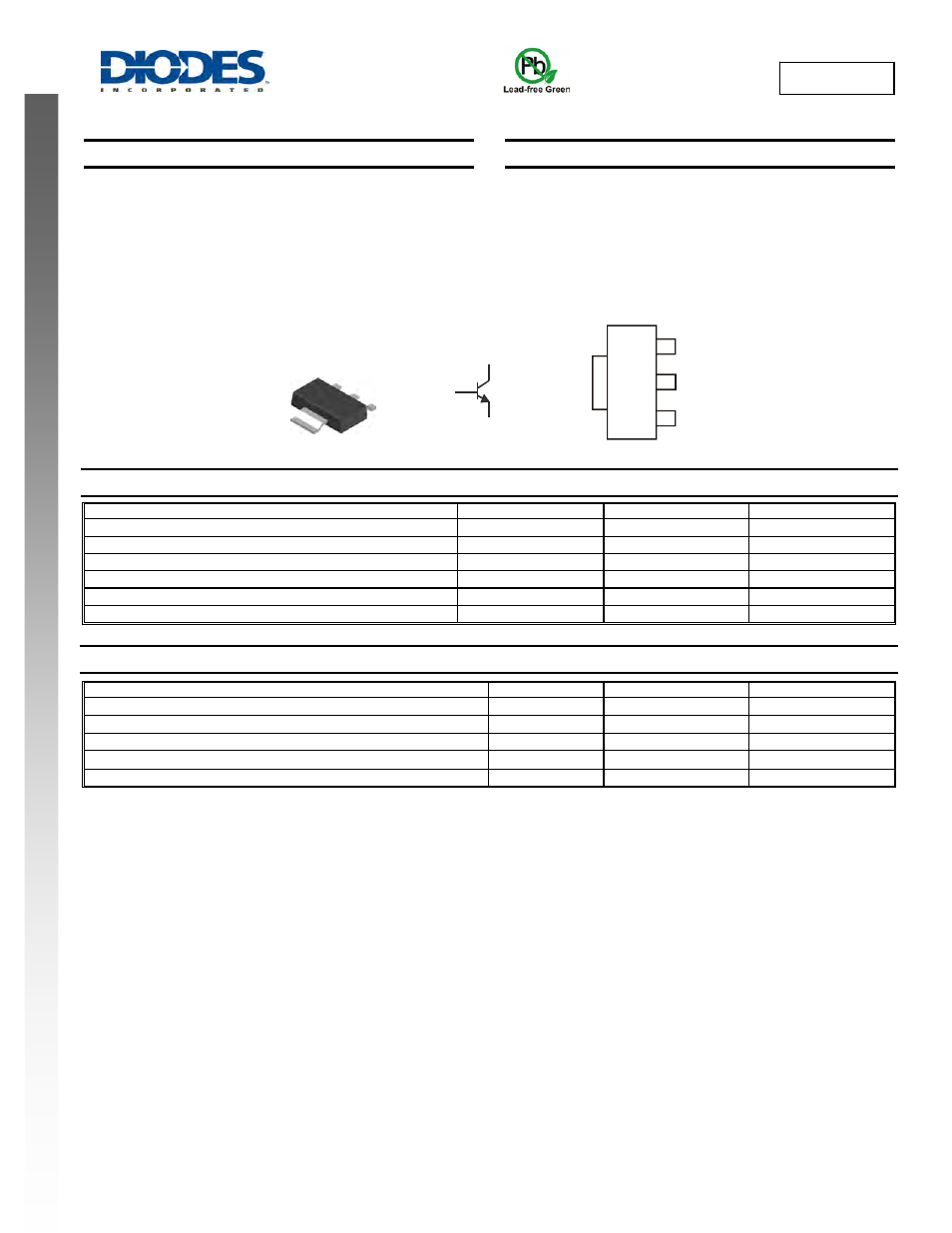
Top View
Device Schematic
Pin Out Configuration
4
3
2
1
C
C
B
E
3
1
2,4
COLLECTOR
EMITTER
BASE