Switching characteristics, Operating characteristics, Package characteristics – Diodes 74LVC126A User Manual
Page 5
74LVC126A
Document number: DS35266 Rev. 3 - 2
5 of 10
June 2012
© Diodes Incorporated
74LVC126A
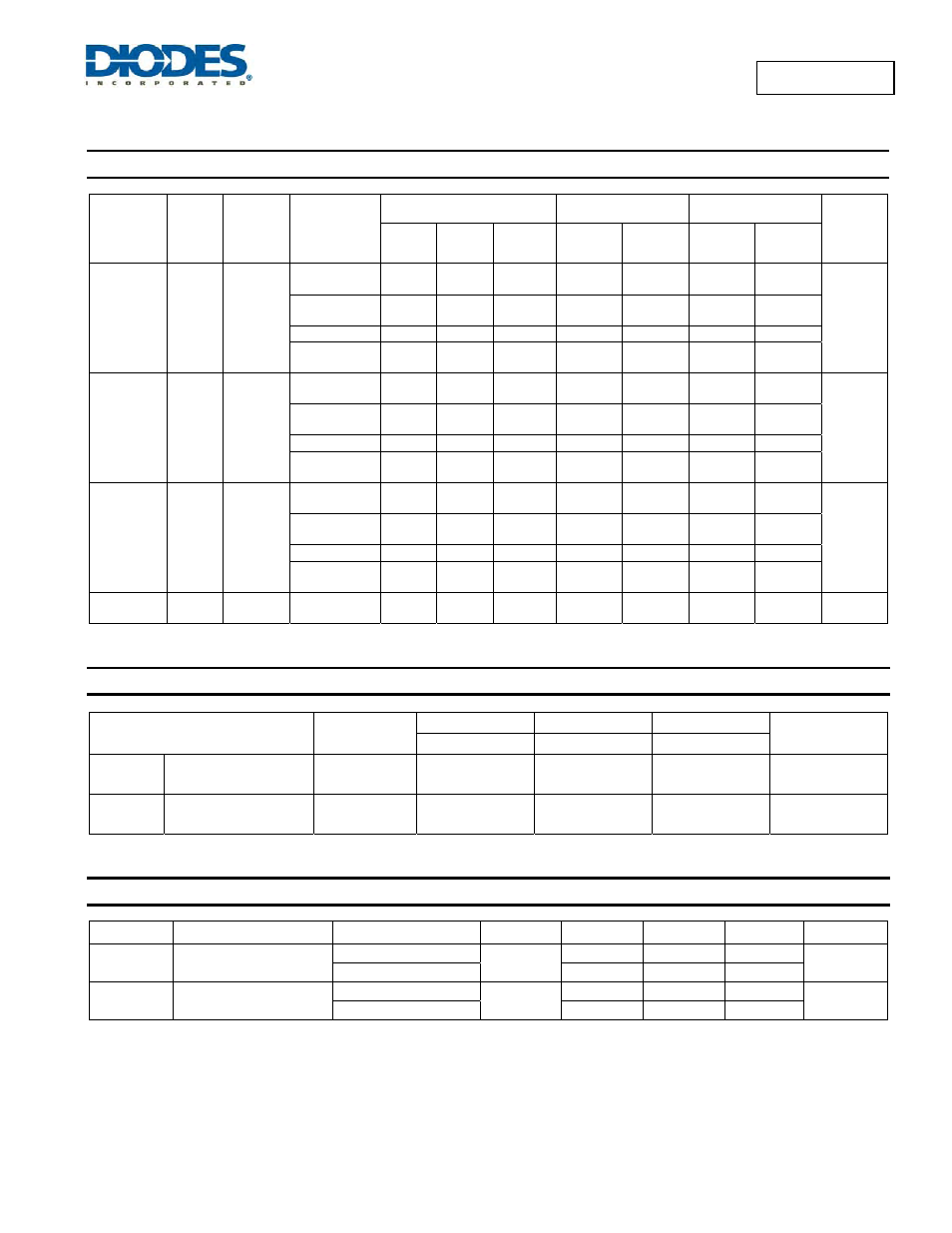
Switching Characteristics
Parameter
From
(Input)
To
(Output)
Test
Conditions
See
Figure 1
T
A
= +25°C
-40°C to +85°C
-40°C to +125°C
Unit
Min Typ Max Min Max Min Max
t
pd
A Y
Vcc = 1.8V
± 0.15V
1.0 4.2 9.3 1.0 9.8 1.0 11.3
ns
Vcc = 2.5V
± 0.2V
1.0 2.7 6.7 1.0 7.2 1.0 9.3
Vcc = 2.7V
1.0
2.9
5.0
1.0
5.2
1.0
6.5
Vcc = 3.3V
± 0.3V
1.0 2.5 4.5 1.0 4.7 1.0 6.0
t
en
OE Y
Vcc = 1.8V
± 0.15V
1.0 4.8 9.5 1.0
10
1.0 11.5
ns
Vcc = 2.5V
± 0.2V
1.0 2.1 7.8 1.0 8.3 1.0 10.4
Vcc = 2.7V
1.0
2.3
6.1
1.0
6.3
1.0
8.0
Vcc = 3.3V
± 0.3V
1.0 2.5 5.5 1.0 5.7 1.0 7.5
t
dis
OE Y
Vcc = 1.8 V
± 0.15V
1.0
4.4
12.1 1.0 12.5 1.0 14.1
ns
Vcc = 2.5V
± 0.2V
1.0 2.7 8.2 1.0 8.7 1.0 10.8
Vcc = 2.7V
1.0
2.7
6.5
1.0
6.7
1.0
8.5
Vcc = 3.3V
± 0.3V
1.0 2.3 5.8 1.0 6.0 1.0 7.5
t
SK(0)
Vcc = 3.3V
± 0.3V
1.0 1.0 1.5 ns
Operating Characteristics
(@T
A
= +25°C, unless otherwise specified.)
Parameter
Test
Conditions
V
CC
= 1.8V
V
CC
= 2.5V
V
CC
= 3.3V
Unit
Typ Typ Typ
C
pd
Power dissipation
capacitance per gate
f = 10 MHz
7.3
11.2
14.9
pF
C
I
Input Capacitance
V
i
= V
CC
– or
GND
4 4 4 pF
Package Characteristics
Symbol
Parameter
Test Conditions
V
CC
Min Typ Max Unit
θ
JA
Thermal Resistance
Junction-to-Ambient
SO-14
(Note 6)
TBD
o
C/W
TSSOP-14
159
θ
JC
Thermal Resistance
Junction-to-Case
SO-14
(Note 6)
TBD
o
C/W
TSSOP-14
25
Note:
6. Test condition for SO-14 and TSSOP-14: Device mounted on FR-4 substrate PC board, 2oz copper, with minimum recommended pad layout.