Preliminary 74lv32a new prod uc t, Pin descriptions, Logic diagram – Diodes 74LV32A User Manual
Page 2: Function table, Absolute maximum ratings
74LV32A
Document number: DS35664 Rev. 1 - 2
2 of 9
October 2013
© Diodes Incorporated
Preliminary
74LV32A
NEW PROD
UC
T
Pin Descriptions
Pin Number
Pin Name
Description
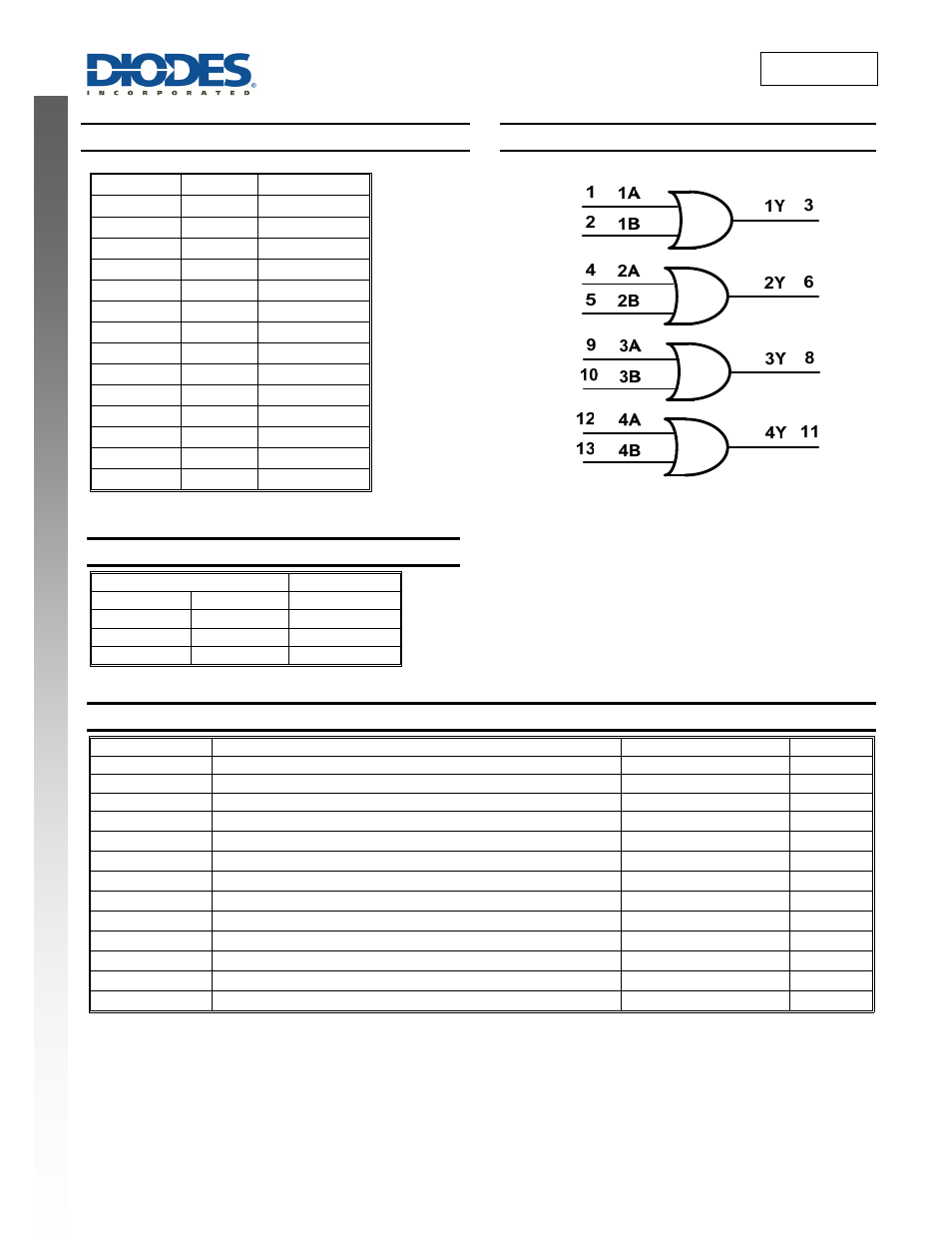
1 1A
Data
Input
2 1B
Data
Input
3 1Y
Data
Output
4 2A
Data
Input
5 2B
Data
Input
6 2Y
Data
Output
7 GND
Ground
8 3Y
Data
Output
9 3A
Data
Input
10 3B
Data
Input
11 4Y
Data
Output
12 4A
Data
Input
13 4B
Data
Input
14 Vcc
Supply
Voltage
Logic Diagram
Function Table
Inputs Output
A B Y
L L L
H X H
X H H
Absolute Maximum Ratings
(Note 4)
(@T
A
= +25°C, unless otherwise specified.)
Symbol
Description
Rating
Unit
ESD HBM
Human Body Model ESD Protection
2
kV
ESD CDM
Charged Device Model ESD Protection
1
kV
ESD MM
Machine Model ESD Protection
200
V
V
CC
Supply Voltage Range
-0.5 to +7.0
V
V
I
Input Voltage Range (Note 4)
-0.5 to +7.0
V
I
IK
Input Clamp Current V
I
< 0V
-20
mA
I
OK
Output Clamp Current V
O
< -0V
-50
mA
I
O
Continuous Output Current -0.5V < V
O
V
CC
+0.5V
±25 mA
I
CC
Continuous Current Through V
cc
50 mA
I
GND
Continuous Current Through GND
-50
mA
T
J
Operating Junction Temperature
-40 to +150
°C
T
STG
Storage Temperature
-65 to +150
°C
P
TOT
Total Power Dissipation
500
mW
Note:
4. Stresses beyond the absolute maximum may result in immediate failure or reduced reliability. These are stress values and device operation should
be within recommend values.