Switching characteristics – Diodes 74HC595 User Manual
Page 6
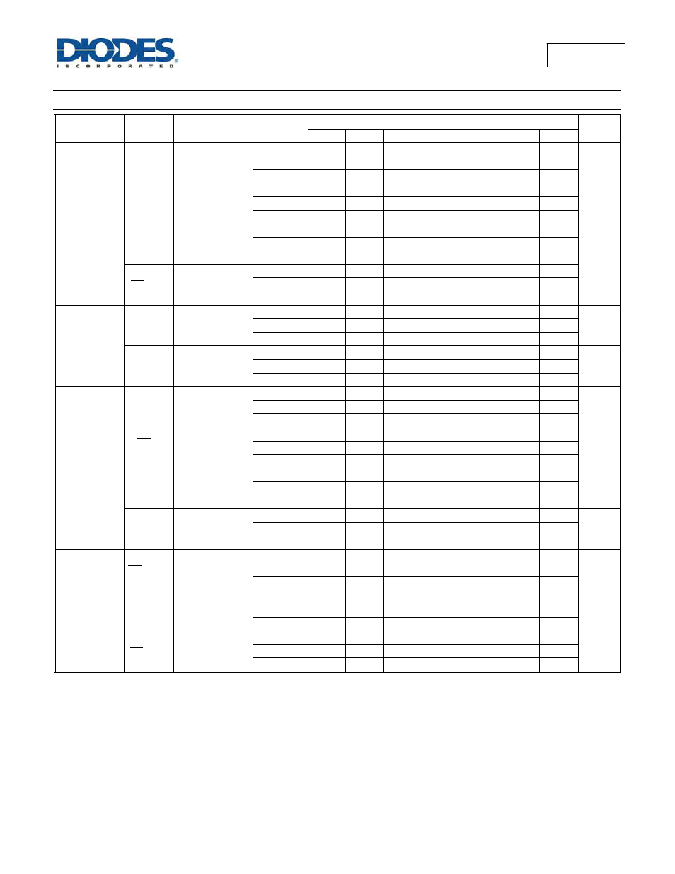
74HC595
Document number: DS35492 Rev. 3 - 2
6 of 11
June 2013
© Diodes Incorporated
74HC595
Switching Characteristics
Symbol /
Parameter
Pins
Test Conditions
V
CC
T
A
= +25°C
-40°C to +85°C
-40°C to +125°C
Unit
Min Typ Max Min Max Min Max
f
MAX
Maximum
Frequency
SHCP or
STCP
Figure 1
2.0V
9
30
4.8
4
MHz
4.5V
30
91
24
20
6.0V
35
108
28
24
t
W
Pulse Width
SHCP
HIGH or
LOW
Figure 1
2.0V
75
17
95
110
ns
4.5V
15
6
19
22
6.0V
13
5
16
19
STCP
HIGH or
LOW
Figure 1
2.0V
75
11
95
110
4.5V
15
4
19
22
6.0V
13
3
16
19
MR LOW
Figure 1
2.0V
75
17
95
110
4.5V
15
6
19
22
6.0V
13
5
16
19
t
SU
Set-up Time
DS to
SHCP
Figure 1
2.0V
50
11
65
75
ns
4.5V
10
4
13
15
6.0V
9
3
11
13
SHCP tp
STCP
Figure 1
2.0V
75
22
95
110
ns
4.5V
15
8
19
22
6.0V
13
7
16
19
t
H
Hold Time
DS to
SHCP
Figure 1
2.0V
3
-6
3
3
ns
4.5V
3
-2
3
3
6.0V
3
-2
3
3
t
REC
Recovery Time
MR to
SHCP
Figure 1
2.0V
50
-19
65
75
ns
4.5V
10
-7
13
15
6.0V
9
-6
11
13
t
PD
Propagation
Delay
SHCP
toQ7S
Figure 1
C
L
=50pF
2.0V
52 160
200
240
ns
4.5V
19 32
40
48
6.0V
15 27
34
41
STCP to
Qn
Figure 1
C
L
=50pF
2.0V
55 175
220
265
ns
4.5V
20 35
44
53
6.0V
16 30
37
45
t
PHL
Propagation
Delay
MR toQ7S
Figure 1
C
L
=50pF
2.0V
47 175
220
265
ns
4.5V
17 35
44
53
6.0V
14 30
37
45
t
EN
Enable Time
OE to Qn
Figure 1
C
L
=50pF
2.0V
47 150
190
225
ns
4.5V
17 30
38
45
6.0V
14 26
33
38
t
DIS
Disable Time
OE to Qn
Figure 1
C
L
=50pF
2.0V
41 150
190
225
ns
4.5V
15 30
38
45
6.0V
12 26
33
38