Functional description and timing diagram, Absolute maximum ratings – Diodes 74HC594 User Manual
Page 3
74AHC594
Document number: DS35484 Rev. 3 - 2
3 of 10
June 2013
© Diodes Incorporated
74HC594
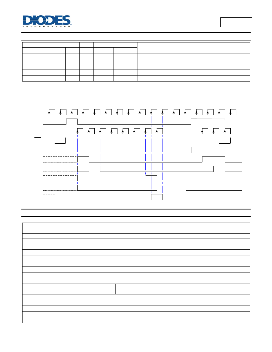
Functional Description and Timing Diagram
Control Input
Output
Function
SHR STR
SHCP STCP DS
Q7S
Qn
L X X X X L
NC Clear
Shift
Register
X L X X X NC
L Clear
Storage
Register
H X
L
H or L
Q6S
NC
Loads DS into shift register stage 0. All Q
S
shifted
H H X
X NC Qs
Contents of shift register moved to starge register all Q
S
-> Q
N
H H
H or L
Q6S
QnS
Shift Register one pulse count ahead of storage register.
H=HIGH voltage state
L=LOW voltage state
=LOW to HIGH transition
X= don’t care – high or low (not floating)
NC= No change
SHCP
DS
STCP
SHR
STR
Q0
Q1
Q6
Q7
Q7S
Absolute Maximum Ratings
(Note 4)
(@T
A
= +25°C, unless otherwise specified.)
Symbol
Description
Rating
Unit
ESD HBM
Human Body Model ESD Protection
2
KV
ESD CDM
Charged Device Model ESD Protection
1
KV
ESD MM
Machine Model ESD Protection
200
V
V
CC
Supply Voltage Range
-0.5 to +7.0
V
V
I
Input Voltage Range
-0.5 to +7.0
V
V
o
Voltage applied to output in high or low state
-0.3 to V
CC
+0.5
V
I
IK
Input Clamp Current V
I
< -0.5V
-20 mA
I
IK
Input Clamp Current VI > Vcc +0.5V
20
mA
I
OK
Output Clamp Current V
O
<-0.5V
-20 mA
I
OK
Output Clamp Current V
O
> V
CC
+ 0.5V
20 mA
I
O
Continuous output current
Q7 standard output
±25
mA
Qn bus driver outputs
±35
mA
I
CC
Continuous current through Vcc
70
mA
I
GND
Continuous current through GND
-70
mA
T
J
Operating Junction Temperature
-40 to +150
°C
T
STG
Storage Temperature
-65 to +150
°C
P
TOT
Total Power Dissipation
500
mW
Note:
4. Stresses beyond the absolute maximum may result in immediate failure or reduced reliability. These are stress values and device operation should be
within recommend values.