Electrical characteristics, Switching characteristics, Operating characteristics – Diodes 74HC125 User Manual
Page 4
74HC125
Document number: DS35326 Rev. 3 - 2
4 of 9
January 2013
© Diodes Incorporated
74HC125
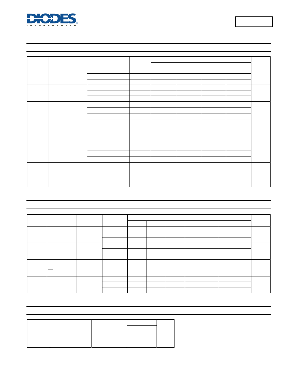
Electrical Characteristics
(@T
A
= +25°C, unless otherwise specified.)
Symbol Parameter Test
Conditions V
CC
T
A
= -40°C to +85°C
T
A
= -40°C to +125°C
Unit
Min Max Min Max
V
IH
High-level Input
Voltage
2.0V
1.5 1.5
V
4.5V
3.15 3.15
6.0V
4.2 4.2
V
IL
Low-level Input
voltage
2.0V
0.5 0.5
V
4.5V 1.35 1.35
6.0V
1.8 1.8
V
OH
High-level Output
Voltage
I
OH
= -20μA
2.0V
1.9 1.9
V
I
OH
= -20μA
4.5V
4.4 4.4
I
OH
= -20μA
6.0V
5.9 5.9
I
OH
= -4.0mA
4.5V 3.84
3.7
I
OH
= -5.2mA
6.0V 5.34
5.2
V
OL
Low-level Output
Voltage
I
OL
= 20μA
2.0V
0.1 0.1
V
I
OL
= 20μA
4.5V
0.1 0.1
I
OL
= 20μA
6.0V
0.1 0.1
I
OL
= 4mA
4.5V 0.33 0.44
I
OL
= 5.2mA
6.0V 0.33 0.44
I
OZ
Z State
Leakage Current
V
O
= 0 to 6.0V
V
I
= GND or 6.0V
6.0V
± 5.0
± 10
μA
I
I
Input Current
V
I
= GND to 5.5V
6.0V
±
1 ±
1
μA
I
CC
Supply Current
V
I
= GND or V
CC
, I
O
= 0
6.0V
20 40
μA
Switching Characteristics
Symbol
Parameter
Test
Conditions
V
CC
T
A
= +25°C
-40°C to +85°C
-40°C to +125°C
Unit
Min Typ. Max
Max
Max
t
PD
Propagation
Delay A
N
to Y
N
Figure 1
C
L
= 50 pF
2.0V — 30
100 125
150
ns
4.5V
—
11
20
25
30
6.0V — 9 17
21
26
t
EN
Enable Time
OE
N
to Y
N
Figure 1
C
L
= 50 pF
2.0V —
41 125
155
190
ns
4.5V
—
15 25
31
38
6.0V
—
12 21
26
32
t
DIS
Disable Time
OE
to Y
N
Figure 1
C
L
= 50 pF
2.0V
—
41 125
155
190
ns
4.5V
—
15 25
31
38
6.0V
—
12 21
26
32
t
t
Transition time
Figure 1
C
L
= 50 pF
2.0V
—
14 60
75
90
ns
4.5V
—
5 12
15
18
6.0V
—
4 10
13
15
Operating Characteristics
(@T
A
= +25°C, unless otherwise specified.)
Parameter Test
Conditions
V
CC
= 6V
Unit
Typ
C
pd
Power Dissipation
Capacitance per Gate
f = 1MHz
22
pF
C
I
Input Capacitance
V
I
= V
CC
– or GND
4 pF