Data sheet, Pin description (continued) – Diodes AUR3852 User Manual
Page 6
Data Sheet
Enhanced Multi-touch Capacitive Touch Screen Controller AUR3852
Feb. 2013 Rev. 1. 0 BCD Semiconductor Manufacturing Limited
6
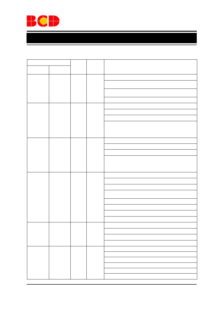
Pin Description (Continued)
Pin Number
Pin
Name
Pin
Type
Pin Function
QFN-6×6-
48
QFN-7×7-
56
15, 18
17, 20
RSTN,
TESTE
N
I
Reset Low Active
Typically connect a resistor to VDD and a capacitor to
VSS
Low asserted and threshold at 0.5×V
DD
. When forced low,
the chip enters into reset condition
This pin should not be connected to any level above V
DD
16 18
P1.3
I/O
Port 1.3 GPIO
8051 P1.3 GPIO
SCL
This pin can also be configured as the SCL signal of the
I
2
C master or I
2
C slave controller. In I
2
C master mode, this
pin should be configured as open-drain output. In I
2
C
slave mode, this pin should be configured as input only
17 19
P1.2
I/O
Port 1.2 GPIO
8051 P1.2 GPIO
SDA
This pin can also be configured as the SDA signal of the
I
2
C master or I
2
C slave controller. In this operation mode,
this pin should also be configured as bi-directional I/O
with open-drain output
19 21
P1.7
I/O
Port 1.7 GPIO
8051 P1.7 GPIO
PINT0.1
This pin can also be configured as the expanded INT0
interrupt
T0 Timer 0 Input
This pin can also be configured as Timer 0 input
External Clock Input
External clock input source
20 25
P1.0
I/O
Port 1.0 GPIO
8051 P1.0 GPIO
DR9
Right driving line 9
21 26
P0.7
I/O
Port 0.7 GPIO
8051 P0.7 GPIO
RXD0
This pin can also be configured as RXD of UART 0
DR8
Right driving line 8