Electrical characteristics – Diodes AP432_A User Manual
Page 3
AP432/AP432A
Document number: DS31003 Rev. 18 - 2
3 of 15
September 2012
© Diodes Incorporated
AP432/AP432A
Electrical Characteristics
(@T
A
= +25°C, unless otherwise specified.)
Symbol Parameter
Test
Conditions
Min
Typ
Max
Unit
V
REF
Reference
voltage
V
KA
= V
REF
,
I
KA
= 10mA (Figure 1)
AP432
AP432A
1.227
1.233
1.24
1.252
1.246
V
V
REF
Deviation of reference input voltage over
temperature
(Note 4)
V
KA
= V
REF
, I
KA
= 10mA,
Ta = Full range (Figure 1)
⎯
3.0 20 mV
ΔV
REF
ΔV
KA
Ratio of the change in reference voltage to
the change in cathode voltage
I
KA
= 10mA (Figure 2)
V
KA
= 20 ~ V
REF
⎯
-1.4 -2.0 mV/V
I
REF
Reference input current
R1 = 10K
Ω,R2 = ∞ I
KA
= 10mA (Figure 2)
⎯
1.4 3.5 µA
αI
REF
Deviation of reference input current over
temperature
R1 = 10K
Ω,R2 = ∞ I
KA
= 10mA
T
A
= Full range (Figure 2)
⎯
0.4 1.2 µA
I
KA(MIN)
Minimum cathode current for regulation
V
KA
= V
REF
(Figure 1)
⎯
0.15 0.3 mA
I
KA(OFF)
Off-state
current
V
KA
= 36V, V
REF
= 0V (Figure 3)
⎯
0.1 1.0 µA
|Z
KA
|
Dynamic output impedance
(Note 5)
V
KA
= V
REF
V
KA
= V
REF
ΔI
KA
= 0.1mA ~ 15mA
Frequency
≤
1KHz (Figure 1)
⎯
0.2 0.5
Ω
V
MAX
V
MIN
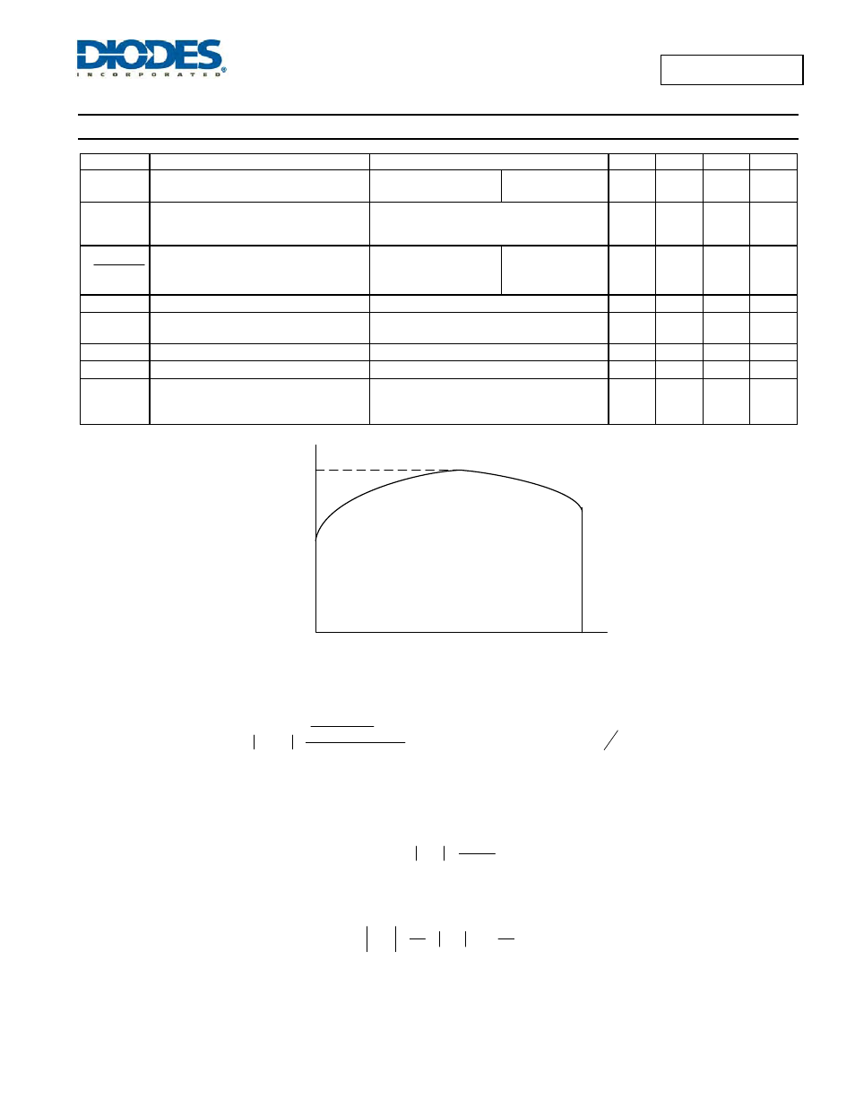
T
I
T
2
Temperature
V
DEV
= V
MAX
- V
MIN
Notes: 6. Deviation of reference input voltage, V
DEV
, is defined as the maximum variation of the reference over the full temperature range.
The average temperature coefficient of the reference input voltage
αV
REF
is defined as:
1
T
2
T
6
10
)
C)
(25
REF
V
DEV
V
(
REF
V
α
−
⋅
°
=
……………………..……………….. (
)
C
ppm
°
Where:
T2 – T1 = full temperature change.
αV
REF
can be positive or negative depending on whether the slope is positive or negative.
Notes: 7. The dynamic output impedance, R
Z
, is defined as:
KA
I
KA
V
KA
Z
Δ
Δ
=
When the device is programmed with two external resistors R1 and R2 (see Figure 2.), the dynamic output impedance of the overall circuit, is
defined as:
)
R2
R1
(1
KA
Z
i
v
'
KA
Z
+
Δ
Δ
=
≈