Recommended operating conditions, Electrical characteristics, A product line of diodes incorporated – Diodes AS339А User Manual
Page 4
AS339/339A
Document number: DS36838 Rev.
2 - 2
4 of 12
January 2014
© Diodes Incorporated
AS339/339A
A Product Line of
Diodes Incorporated
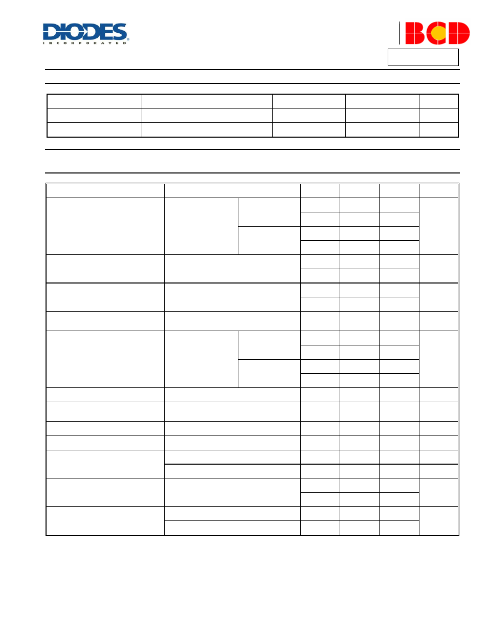
Recommended Operating Conditions
Symbol
Parameter
Min
Max
Unit
V
CC
Supply Voltage
2
36
V
T
A
Operating Temperature Range
-40
+85
C
Electrical Characteristics
(Limits in standard typeface are for T
A
= +25
o
C, bold typeface applies over T
A
= -40
o
C to +85
o
C (Note 3),
V
CC
= 5V, GND = 0V, unless otherwise specified.)
Notes:
3. Limits over the full temperature are guaranteed by design, but not tested in production.
4. The input common-mode voltage of either input signal voltage should not be allowed to go negatively by more than 0.3V (at +25
o
C). The upper end of the
common-mode voltage range is V
CC
-1.5V (at +25
o
C), but either or both inputs can go to +36V without damages, independent of the magnitude of the V
CC.
Parameter
Conditions
Min
Typ
Max
Unit
Input Offset Voltage
V
O
= 1.4V, R
S
=
0Ω,
V
CC
from 5V to 30V
AS339
–
2
5
mV
–
–
7
AS339A
–
2
3
–
–
5
Input Bias Current
I
IN
+
or I
IN
-
with output in Linear Range, V
CM
= 0V
–
25
250
nA
–
–
400
Input Offset Current
I
IN
+
- I
IN
-
, V
CM
= 0V
–
5.0
50
nA
–
–
200
Input Common Mode Voltage Range
(Note 4)
V
CC
= 30V
0
–
V
CC
-1.5
V
Supply Current
R
L
= ∞
V
CC
= 5V
–
0.9
2.0
mA
–
–
3.0
V
CC
= 30V
–
1.2
2.5
–
–
3.5
Voltage Gain
R
L
≥ 15kΩ, V
CC
= 15V, V
O
= 1V to 11V
50
200
–
V/mV
Large Signal Response Time
V
IN
= TTL Logic Swing, V
REF
= 1.4V
V
RL
= 5V, R
L
=
5.1kΩ
–
200
–
ns
Response Time
V
RL
= 5V, R
L
=
5.1kΩ
–
1.3
–
µs
Output Sink Current
V
IN
-
= 1V, V
IN
+
= 0, V
O
= 1.5V
6.0
16
–
mA
Output Leakage Current
V
IN
-
= 0V, V
IN
+
= 1V, V
O
= 5V
–
0.1
–
nA
V
IN
-
= 0V, V
IN
+
= 1V, V
O
= 30V
–
–
1
µA
Saturation Voltage
V
IN
-
= 1V, V
IN
+
= 0, I
SINK
≤ 4mA
–
200
400
mV
–
–
500
Thermal Resistance (Junction to
Case)
SOIC-14
–
51.93
–
o
C/W
DIP-14
–
35.00
–