Diodes AS331 User Manual
Page 4
LOW POWER LOW OFFSET VOLTAGE SINGLE COMPARATOR AS331
Data Sheet
4
May. 2010 Rev. 1. 4
BCD Semiconductor Manufacturing Limited
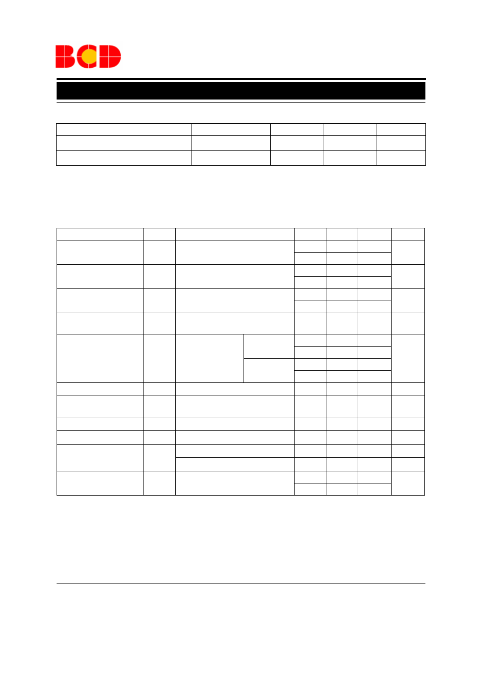
Parameter
Symbol
Min
Max
Unit
Supply Voltage
V
CC
2
36
V
Operating Ambient Temperature Range
T
A
-40
85
o
C
Recommended Operating Conditions
Electrical Characteristics
Parameter
Symbol Conditions
Min
Typ
Max
Unit
Input Offset Voltage
V
OS
V
OUT
=1.4V, V
CC
=5 to 30V
1
5
mV
7.0
Input Bias Current
I
B
I
IN
+ or I
IN
- with output in linear range,
V
CM
=0V
25
250
nA
400
Input Offset Current
I
IO
I
IN
+-I
IN
-, V
CM
=0V
5
50
nA
200
Input Common Mode
Voltage Range (Note 4)
V
CC
=30V
0
V
CC
-1.5
V
Supply Current
I
CC
R
L=
∞
V
CC
=5V
0.4
1.0
mA
2.0
V
CC
=30V
0.5
1.7
3.0
Voltage Gain
G
V
V
CC
=15V, R
L
≥15kΩ, V
OUT
=1 to 11V
50
200
V/mV
Large Signal Response
Time
V
IN
=TTL Logic Swing, R
L
=5.1k
Ω
200
ns
Response Time
R
L
=5.1k
Ω
1.3
µs
Output Sink Current
I
SINK
V
IN
-=1V, V
IN
+=0V, V
OUT
=1.5V
6.0
16
mA
Output Leakage Current
I
LEAK
V
IN
-=0V, V
IN
+=1V, V
OUT
=5V
0.1
nA
V
IN
-=0V, V
IN
+=1V, V
OUT
=30V
1
µA
Saturation Voltage
V
SAT
V
IN
-=1V, V
IN
+=0V, I
SINK
≤4mA
200
400
mV
500
V
CC
=5V, GND=0V, T
A
=25
o
C, unless otherwise specified. Bold typeface applies over T
A
=-40 to 85
o
C (Note 3)
Note 3: These specifications are limited to -40
o
C
≤T
A
≤85
o
C. Limits over temperature are guaranteed by design, but
not tested in production.
Note 4: The input common mode voltage of either input signal voltage should not be allowed to go negatively by
more than 0.3V (at 25
o
C
). The upper end of the common mode voltage range is V
CC
-1.5V (at 25
o
C
), but either or
both inputs can go to +36V without damages, independent of the magnitude of the V
CC
.