Ah1892, New prod uc t, Absolute maximum ratings – Diodes AH1892 User Manual
Page 3: Recommended operating conditions, Electrical characteristics
AH1892
PROGRAMMABLE MICROPOWER OMNIPOLAR
HALL-EFFECT SENSOR SWITCH
AH1892
Document number: DS35092 Rev. 1 - 2
3 of 11
May 2012
© Diodes Incorporated
NEW PROD
UC
T
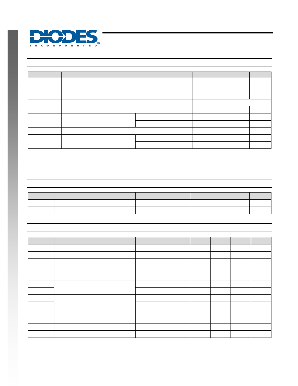
Absolute Maximum Ratings
(T
A
= +25
°C, Note 5)
Symbol
Characteristics
Values
Unit
V
DD
Supply Voltage (Note 6)
6
V
V
DD REV
Reverse Supply Voltage
-0.3
V
I
OUTPUT
Output current (source and sink)
2.5
mA
B
Magnetic Flux Density
Unlimited
Ts
Storage Temperature Range
-65 to +150
°C
P
D
Package Power Dissipation
U-WLB0707-4
160
mW
SOT553
230
mW
T
J
Maximum Junction Temperature
150
°C
ESD
Human Body Model ESD
V
DD
, GND and OUT pins
8
kV
BSEL pin
6
kV
Notes:
5. Stresses greater than the 'Absolute Maximum Ratings' specified above, may cause permanent damage to the device. These are stress ratings
only; functional operation of the device at these or any other conditions exceeding those indicated in this specification is not implied. Device
reliability may be affected by exposure to absolute maximum rating conditions for extended periods of time
6. The absolute maximum V
DD
of 6V is a transient stress rating and is not meant as a functional operating condition. It is not recommended to
operate the device at the absolute maximum rated conditions for any period of time.
Recommended Operating Conditions
Symbol
Characteristics
Conditions
Rating
Unit
V
DD
Supply Voltage
Operating
1.6 to 3.6
V
T
A
Operating Temperature Range
Operating
-40 to +85
°C
Electrical Characteristics
(T
A
= +25
°C, V
DD
= 1.8V, unless otherwise specified.)
Symbol
Characteristics
Conditions
Min
Typ
Max
Unit
V
OL
Output low voltage (on)
I
OUT
= 1mA
0.1
0.2
V
V
OH
Output high voltage (off)
I
OUT
= -1mA
V
DD
-0.2 V
DD
-0.1
V
BLsel
Band select low band
0
0.5
V
BHsel
Band select high band
1.4
3.6
V
R
U_BSEL
BSEL pin internal pull-up resistor
(Note 7)
50
k
Ω
I
DD
(awake)
Supply current
During ‘awake’ period
2.1
mA
I
DD
(sleep)
During ‘sleep’ period
2.5
µA
I
DD
(avg)
Average cupply current
V
DD
= 1.8V
4.3
8.0
µA
I
DD
(avg) V
DD
= 3.6V
7.2
13.0
µA
Tawake
Awake active pulse width
(Note 8)
50
100
µs
Tperiod
Awake period
(Note 8)
50
100
ms
D.C. Duty
cycle
0.1
%
TBand
Band transition time
( Note 9)
100.0
200.1
ms
Notes:
7. BSEL pin internal pull-up resistor is only active during AWAKE time.
8. When power is initially on, the operating V
DD
(1.6V to 3.6V) must be applied to guarantee the output sampling.
The output state is valid after the second operating phase (typical 100ms).
9. Transition time varies dependant on the timing of BSEL activation during the sleep and awake phases.