Ah375 – Diodes AH375 User Manual
Page 2
AH375
SINGLE PHASE HALL EFFECT LATCH
AH375
Document number: DS31172 Rev. 6 - 2
2 of 9
July 2010
© Diodes Incorporated
Pin Descriptions
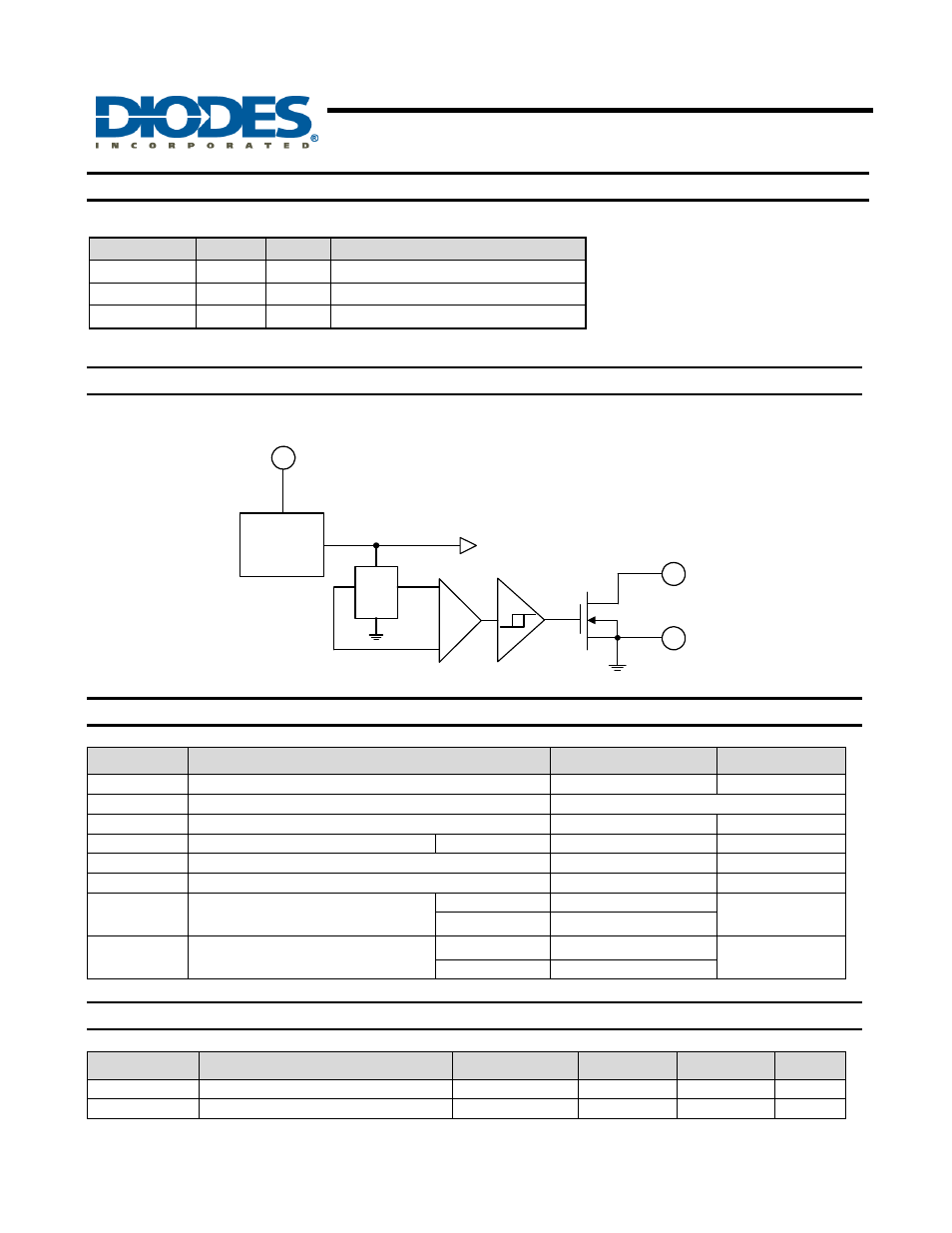
Functional Block Diagram
Regulator
Hall
plate
Amp
2
GND
OUT
3
2
V
dd
1
Absolute Maximum Ratings
(T
A
= 25
°C)
Symbol
Characteristics
Values
Unit
Vdd Supply
Voltage
20
V
B
Magnetic Flux Density
Unlimited
V
DS
Output
OFF
Voltage
30
V
Id Output
“On”
Current
Continuous
25
mA
T
S
Storage
Temperature
Range
-65~+150
°C
T
J(MAX)
Maximum Junction Temperature
150
°C
P
D
Package Power Dissipation
SIP-3L 550
mW
SC59 230
θ
JC
Thermal
Resistance
SIP-3L 227
°C/W
SC59 543
Recommended Operating Conditions
Symbol
Parameter
Conditions
Min
Max
Unit
Vdd
Supply Voltage (Note 2) Operating
2.2
20
V
T
A
Operating Ambient Temperature
Operating
-40
125
°C
Notes: 2. The output of IC will be switched after the supply voltage is over 2.2V, but the magnetic characteristics won't be normal until the
supply is over 2.5V.
Pin Name
P/I/O
Pin #
Description
Vdd
P 1
Positive Power Supply
GND
P 2
Ground
OUT
O 3
Output Pin