Data sheet ordering information – Diodes AP3608E User Manual
Page 5

EIGHT-CHANNEL CONSTANT CURRENT SINK WITH CURRENT MATCH AP3608E
5
Mar. 2011 Rev. 1. 5
BCD Semiconductor Manufacturing Limited
Data Sheet
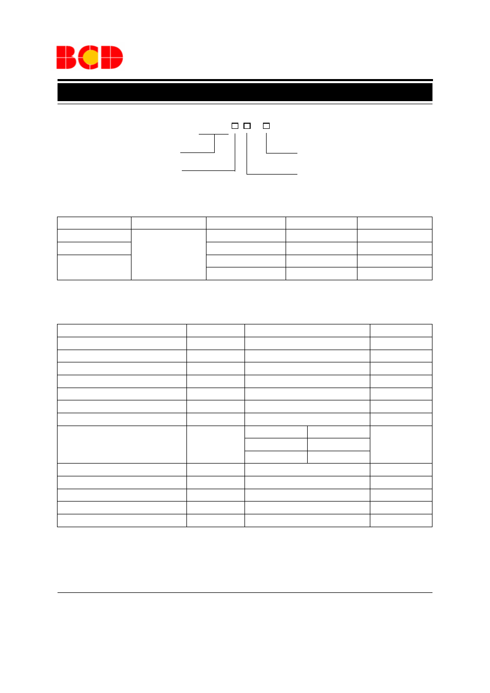
Ordering Information
Package
Temperature Range
Part Number
Marking ID
Packing Type
QFN-4
×
4-24
-40 to 85
o
C
AP3608EFNTR-G1
B3B
Tape & Reel
TSSOP-20(EDP)
AP3608EGTR-G1
AP3608EG-G1
Tape & Reel
SOIC-20
AP3608EM-G1
AP3608EM-G1
Tube
AP3608EMTR-G1
AP3608EM-G1
Tape & Reel
Circuit Type
Package
FN: QFN-4
×
4-24
G1: Green
AP3608E -
TR: Tape and Reel
BCD Semiconductor's Pb-free products, as designated with "G1" suffix in the part number, are RoHS compliant and green.
Parameter Symbol
Value
Unit
Input Voltage
V
CC
-0.3 to 6
V
ISET Pin Voltage
V
ISET
-0.3 to 6
V
EN Pin Voltage
V
EN
-0.3 to 6
V
Feedback Pin Voltage
V
FB
-0.3 to 6
V
SDB Pin Voltage
V
SDB
-0.3 to 6
V
PWM Pin Voltage
V
PWM
-0.3 to 6
V
Voltage per Channel (Note 3)
V
CHX
-0.3 to 40
V
Thermal Resistance
(Junction to Ambient, No Heat Sink)
θ
JA
QFN-4
×4-24
60
o
C/W
TSSOP-20(EDP)
35 (Note 2)
SOIC-20
87
Operating Junction Temperature
T
J
150
o
C
Storage Temperature Range
T
STG
-65 to 150
o
C
Lead Temperature (Soldering, 10sec)
T
LEAD
260
o
C
ESD (Machine Model)
200
V
ESD (Human Body Model)
6000
V
Note 1: Stresses greater than those listed under "Absolute Maximum Ratings" may cause permanent damage to the device.
These are stress ratings only, and functional operation of the device at these or any other conditions beyond those indicated
under "Recommended Operating Conditions" is not implied. Exposure to "Absolute Maximum Ratings" for extended periods
may affect device reliability.
Note 2: The chip is soldered to 60mm
2
(4mm
×15mm) copper (top side solder mask) of 1oz. on PCB with 8×0.5mm vias.
Note 3: Breakdown voltage.
Absolute Maximum Ratings (Note 1)
G: TSSOP-20(EDP)
Blank: Tube
M: SOIC-20
