Ap5725 – Diodes AP5725 User Manual
Page 4
AP5725
WHITE LED STEP-UP CONVERTER
AP5725
Document number: DS31844 Rev. 3 - 2
4 of 17
July 2010
© Diodes Incorporated
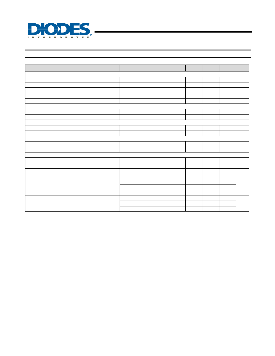
Electrical Characteristics
(V
IN
= 3.6V, T
A
= 25°C, unless otherwise specified.)
Symbol
Parameter
Conditions
Min
Typ.
Max
Unit
System Supply Input
V
IN
Operating Input Voltage
2.7
-
5.5
V
UVLO
Under Voltage Lockout
-
2.2
2.4
V
Under Voltage Lockout Hysteretic
-
85
-
mV
I
Q
Quiescent Current
FB=0.35V, No Switching
-
500
-
μA
I
SD
Shutdown
Current
V
EN
< 0.4V
-
0.1
1
μA
Oscillator
F
OSC
Operation
Frequency
1 1.2 1.4 MHz
Dmax
Maximum Duty Cycle
86
90
-
%
Reference Voltage
V
FB
Feedback
Voltage
0.225 0.25 0.275 V
I
FB
FB Pin Bias Current
10
45
100
nA
MOSFET
Rds(on) On Resistance of MOSFET
-
0.95
1.2
Ω
I
OCP
Switching Current Limit
Normal Operation
-
750
-
mA
Control and Protection
EN Voltage
High
ON
1.5 -
- V
EN Voltage
Low
OFF
-
- 0.4 V
I
EN
EN Pin Pull Low Current
-
4
6
μA
OVP
OVP Threshold
26
30
34
V
θ
JA
Thermal Resistance Junction-to-
Ambient
SOT26 (Note 2)
162
o
C/W
TSOT23-6 (Note 2)
152
DFN2020C-6 (Note2)
200
θ
JC
Thermal Resistance Junction-to-
Case
SOT26 (Note 2)
36
o
C/W
TSOT23-6 (Note 2)
32
DFN2020C-6 (Note 2)
30
Notes: 2. Test condition for SOT26, TSOT23-6 and DFN2020C-6: Device mounted on FR-4 substrate, single-layer PC board, 2oz copper,
with minimum recommended pad layout