Ap3156, Electrical characteristics – Diodes AP3156 User Manual
Page 5
AP3156
HIGH EFFICIENCY 1X/1.5X/2X CHARGE PUMP
FOR WHITE LED APPLICATIONS
AP3156 Rev. 1
5 of 15
SEPTEMBER 2009
©
Diodes Incorporated
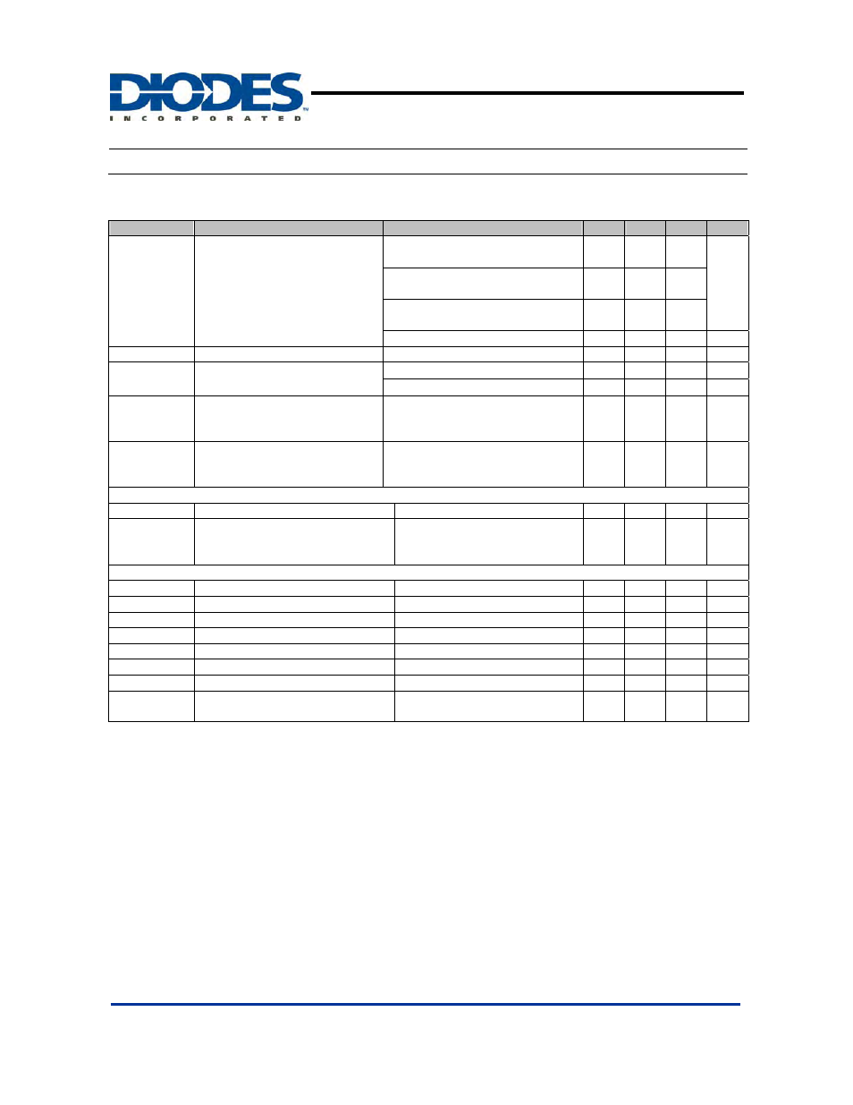
Electrical Characteristics
C
IN
= C
OUT
= C
1
= C
2
= 1.0µF; T
A
= 25°C, V
IN
= 3.5V. Unless otherwise noted.
Symbol
Parameter
Test Conditions
Min Typ. Max
Unit
I
Q
Quiescent
Current
1X Mode, 3.0
≤
V
IN
≤
5.5, Active,
No Load Current
0.3 1
mA
1.5X Mode, 3.0
≤
V
IN
≤
5.5, Active,
No Load Current
2.0 3
2X Mode, 3.0
≤
V
IN
≤
5.5, Active,
No Load Current
1.5 3
50µA Setting, 1X Mode
50
µA
I
SHDN
Shutdown Current
SDI = 0
1
µA
I
DX
I
SINK
Current Accuracy
(Note 4)
I
SET
= 20mA (Note 5), T
A
= 25
°C
18.6 20 21.4 mA
I
SET
= 4mA (Note 5), T
A
= 25
°C
3.6 4 4.4 mA
I
D-Match
Current Matching Between Any
Two Current Sink Inputs
(Note 6)
V
F
:
D1:D6 = 3.6V
0.5 %
V
TH
1X to 1.5X or 1.5X to 2X
Transition Threshold at Any
I
SINK
Pin
I
SET
= 25mA
150
mV
Charge Pump Section
T
SS
Soft-Start
Time
40 µs
F
CLK
Clock
Frequency
0.5/
1/
2
MHz
SDI
V
SDI(L)
SDI
Threshold
Low
V
IN
= 2.7V
0.4
V
V
SDI(H)
SDI
Threshold
High
V
IN
= 5.5V
1.4
V
T
SLO
SDI
Low
Time
0.3 50 µs
T
SHI
SDI High Time
0.05
50
µs
T
OFF
SDI
Off
Timeout
256
µs
T
SEP
SDI Valid Sequence Timeout
256
µs
I
SDI
SDI Input Leakage
-1
1
µA
θ
JA
Thermal Resistance
Junction-to-Ambient
QFN4040-16
(Note
7)
46
o
C/W
Notes: 4. Determined by the average current levels of all active channels
5. Sequence setting set to give nominal 20mA max output current and 4mA output current.
6. Defined as the deviation of any sink current from the average of all active current channels
7. Device mounted on FR-4 substrate, 2"*2", 2oz, copper, double-sided PC board,