Al3157, Ne w produc t absolute maximum ratings, Recommended operating conditions – Diodes AL3157 User Manual
Page 3: Electrical characteristics
AL3157
HIGH EFFICIENCY 1x/2x CHARGE PUMP LED DRIVER
FOR SMALL SCREEN BACKLIGHTING AND FLASHLIGHT
AL3157
Document number: DS35116 Rev. 1 - 2
3 of 9
March 2011
© Diodes Incorporated
N
E
W
PRODUC
T
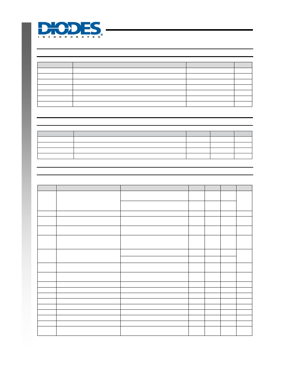
Absolute Maximum Ratings
(Note 2)
Symbol
Description
Rating
Unit
ESD HBM
Human Body Model ESD Protection
2
kV
ESD MM
Machine Model ESD Protection
200
V
V
IN
Input Voltage
-0.3 to 6
V
V
EN1,2,3
EN1, EN2, EN3 to GND Voltage
-0.3 to V
IN
+0.3
V
I
OUT
Maximum DC Output Current
300
mA
T
J
Operating Junction Temperature Range
125
°C
T
LEAD
Maximum Soldering Temperature (at leads, 10 sec)
300
°C
Notes: 2. Exceeding Absolute Maximum Ratings will cause permanent damage to the device.
Recommended Operating Conditions
Symbol
Parameter
Min
Max
Unit
V
IN
Input
Voltage
2.7 5.5 V
V
ENL(1, 2)
EN1,2 Threshold Low
0
0.4
V
V
ENH(1,2)
EN1,2, Threshold High
1.4
V
IN
V
T
A
Operating Ambient Temperature
-40
85
°C
Electrical Characteristics
V
IN
= 4V, C
IN
= C
OUT
= 2.2µF, C
1
= 1µF; T
A
= 25°C unless otherwise noted.
Symbol
Parameter
Test Conditions
Min
Typ.
Max
Unit
I
Q
Quiescent
Current
1x Mode, 3.0≤V
IN
≤5.5, Active,
No Load Current
0.3
0.6
mA
2x Mode, 3.0≤V
IN
≤5.5, Active,
No Load Current
2 5
I
SHDN
Shutdown Current
EN1, EN2 = 0
1
µA
I
D2~4
Backlight LED Drive Sink Current
Accuracy (Note 3)
I
DX
= 30mA
28.5
30
31.5
mA
I
D1
Flash/light LED Drive Sink Current
Accuracy (Note 3)
I
D1
= 210mA
199.5
210
220.5
mA
I
D-Match
Current Matching Between Any
Two Backlight LED Drive Current
Sink Outputs (Note 4)
V
F
: D2:D4 = 4V
1
2
%
R
out
Charge Pump V
OUT
Open Loop
Resistance
1x
mode
0.5
Ω
2x
mode
4.5
V
TH-Dx
1x to 2x Transition Threshold at
D2, D3 and D4 Pins
I
D
= 30mA
150
mV
V
TH-D1
1x to 2x Transition Threshold at D1
Pin
I
D1
=
210mA
150 mV
V
HS
Mode
Transition
Threshold
500 mV
t
SS
Soft-Start
Time
100 µs
f
SW
Switching
Frequency
1.2 MHz
t
EN1,2
EN1,2
Off
Timeout
20
ms
UVLO V
IN
Under-Voltage
Lockout
1.8 2 2.2 V
I
EN1,2
EN1, 2 Input Leakage
-1
1
µA
T
SHDN
Thermal Shutdown Protection
160
o
C
T
HYS
Thermal Shutdown Hysteresis
10
o
C
θ
JA
Thermal Resistance
Junction-to-Ambient
U-DFN3030-12
(Note
5)
55.29
o
C/W
Notes:
3.
Determined by the mean of channels 2,3 and 4 currents, EG (I
D2
+ I
D3
+ I
D4
)/3
4. Determined by the maximum sink current (MAX), the minimum sink current (MIN), and the average sink current (AVG). Two matching
numbers are calculated as (MAX-AVG)/AVG and (AVG-MIN)/AVG. The largest number of the two (worst case) is as the matching data.
5. Device mounted on FR-4 substrate, 2"*2", 2oz, copper, double-sided PC board.