Al3157, Ne w produc t pin descriptions, Functional block diagram – Diodes AL3157 User Manual
Page 2
AL3157
HIGH EFFICIENCY 1x/2x CHARGE PUMP LED DRIVER
FOR SMALL SCREEN BACKLIGHTING AND FLASHLIGHT
AL3157
Document number: DS35116 Rev. 1 - 2
2 of 9
March 2011
© Diodes Incorporated
N
E
W
PRODUC
T
Pin Descriptions
Pin Name
Pin Number
Description
EN2
1
Enable Pin 2: Controls outputs D2, D3 and D4
PGND
2
Charge Pump Switch Ground: Connect to GND
C
N
3
Negative Terminal of Flying Capacitor
V
IN
4
Input Power Supply. Decouple with a 2.2µF capacitor between this pin and ground.
C
P
5
Positive Terminal of Flying Capacitor
V
OUT
6
Charge pump output to drive D1~D4 load circuit. Decouple with a 2.2µF capacitor between
this pin and ground.
D4
7
Current sink input #4. Drive up to 30mA LED current. Connect to V
OUT
when un-used.
D3
8
Current sink input #3. Drive up to 30mA LED current. Connect to V
OUT
when un-used.
GND 9
Ground
D2
10
Current sink input #2. Drive up to 30mA LED current. Connect to V
OUT
when un-used.
EN1
11
Enable Pin 1: Controls output D1
D1
12
Current sink input #1. Drive up to 210mA LED current. Connect to V
OUT
when un-used.
EP
EP PAD
Exposed Pad (bottom). Connect to GND directly underneath the package.
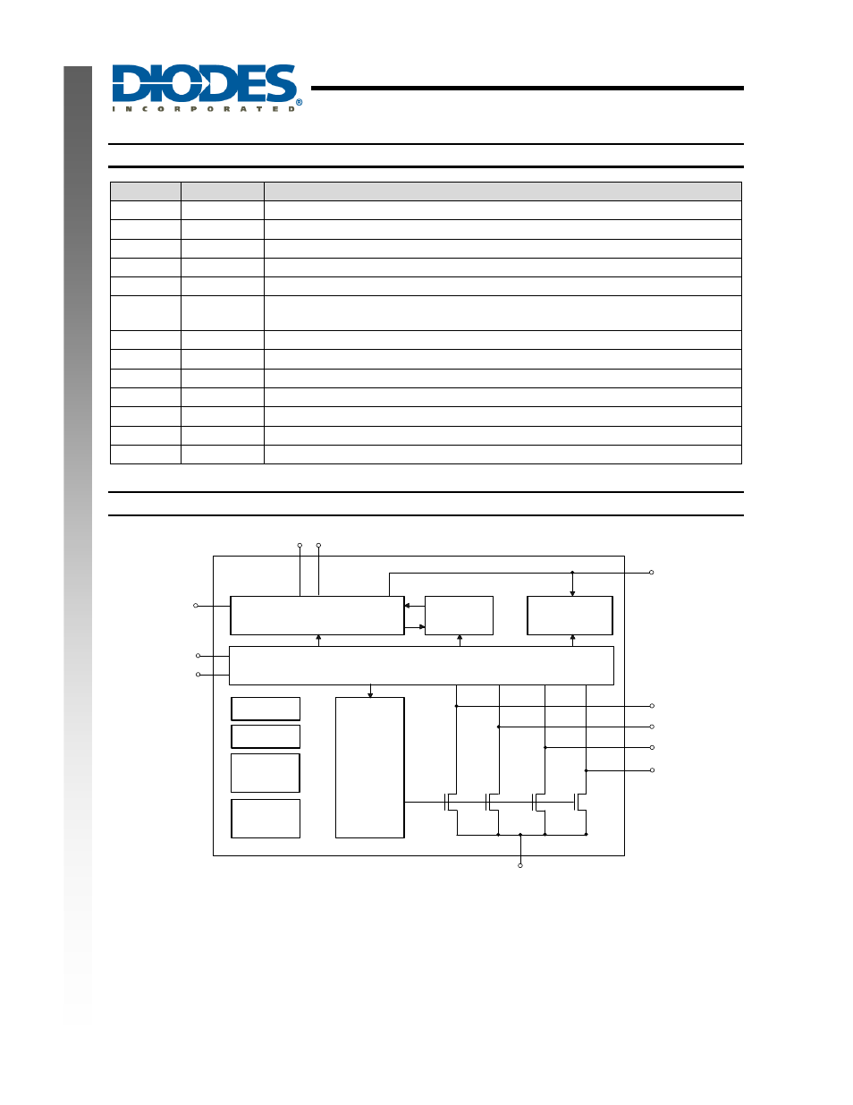
Functional Block Diagram
SHORT
CIRCUIT
PROTECTION
C
N
C
P
V
IN
GND
CURRENT
CONTROL
CHARGE PUMP
SWITCHES
V
OUT
OVER
VOLTAGE
PROTECTION
EN1
UNDER
VOLTAGE
LOCKOUT
BANDGAP
OSCILLATOR
OVER
TEMPERATURE
PROTECTION
D1
D2
D3
D4
EN2
DIGITAL CONTROL BLOCK