Ap1694, New prod uc t functional block diagram, Absolute maximum ratings – Diodes AP1694 User Manual
Page 3
AP1694
Document number: DS36522 Rev.
2 - 2
3 of 9
December 2013
© Diodes Incorporated
AP1694
A Product Line of
Diodes Incorporated
NEW PROD
UC
T
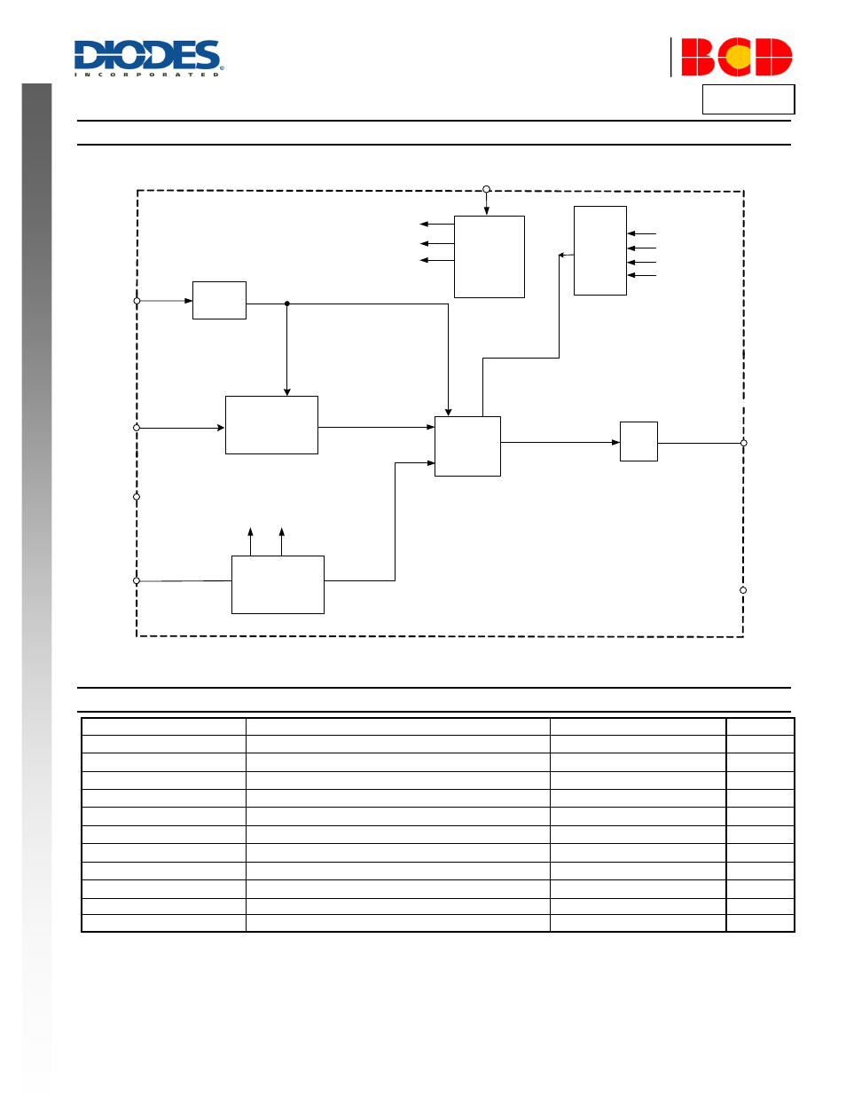
Functional Block Diagram
Regulator&
Bias
Tons
Detector
Tons
Power_EN
Driver
FB
VCC
OUT
PFM
R
S
Q
Vref
CC_CTRL
TONP_CTRL
CS
GND
Vdd
Protection
& Latch
PRO
CS_OCP
FB_CV
FB_OVP
VCC_OVP
Logic
Set Initial Tonp
Constant Turn-on
Time Generation
Vcsmax
Vcs_valley
RI
SGND
5
2
3
4
6
7
8
Absolute Maximum Ratings
(Note 4) (@T
A
= +25°C, unless otherwise specified.)
Symbol Parameter
Rating
Unit
V
CC
Power Supply Voltage
-0.3 to 35
V
I
OUT
Driver Output Current
150
mA
V
CS
Voltage at CS to GND
-0.3 to 7
V
V
FB
FB Input Voltage
-40 to 10
V
T
J
Operating Junction Temperature
-40 to +150
°C
T
STG
Storage Temperature
-65 to +150
°C
T
LEAD
Lead Temperature (Soldering, 10 sec)
+300
°C
P
D
Power Dissipation (T
A
= +50
°C)
0.65 W
θ
JA
Thermal Resistance (Junction to Ambient)
160
°C/W
–
ESD (Human Body Model)
2000
V
–
ESD (Charged-device Model)
±1000
V
Note: 4. Stresses greater than those listed under “Absolute Maximum Ratings” may cause permanent damage to the device. These are stress ratings only, and
functional operation of the device at these or any other conditions beyond those indicated under “Recommended Operating Conditions” is not implied.
Exposure to “Absolute Maximum Ratings” for extended periods may affect device reliability.