Diodes AZ39151 User Manual
Page 6
6
Dec. 2011 Rev. 1. 9
BCD Semiconductor Manufacturing Limited
Data sheet
1.5A ULTRA LOW DROPOUT LINEAR REGULATOR AZ39151
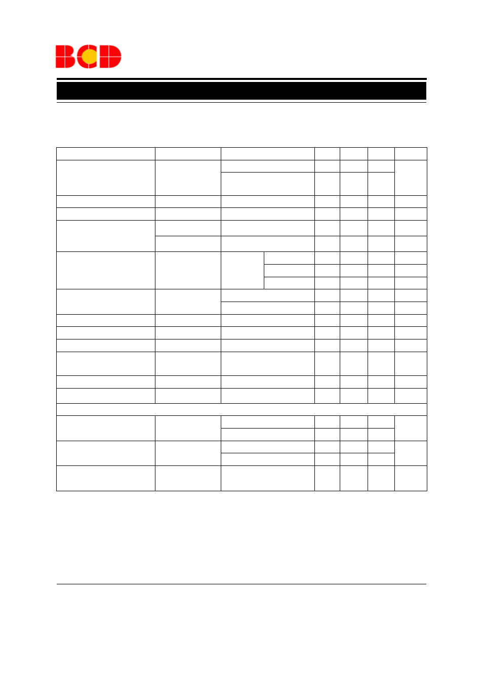
Electrical Characteristics
Parameter
Symbol
Conditions
Min
Typ
Max
Unit
Output Voltage
V
OUT
-1
1
%
10mA
≤I
OUT
≤1.5A,
V
OUT
+1V
≤V
IN
≤13.5V
-2
2
Line Regulation
V
RLINE
V
OUT
+1V
≤V
IN
≤13.5V
3
25
mV
Load Regulation
V
RLOAD
10mA
≤I
OUT
≤1.5A
10
50
mV
Output Voltage
Temperature Coefficient
(Note 2)
∆V
OUT
/
∆T
100
500
µV/
o
C
(∆V
OUT
/V
OUT
)/
∆T
20
100
ppm/
o
C
Dropout Voltage (Note 3)
V
DROP
∆V
OUT
=1%
I
OUT
=100mA
80
200
mV
I
OUT
=750mA
260
mV
I
OUT
=1.5A
375
700
mV
Ground Current
I
GND
I
OUT
=750mA
5
10
mA
I
OUT
=1.5A
17
34
mA
Standby Current
I
STD
V
IN
=13.5V, V
EN
=0V
130
220
µA
Dropout Ground Pin Current
I
GND(DO)
V
IN
≤V
OUT(NOMINAL)
-0.5V
5
mA
Short Circuit Current
I
SHORT
V
OUT
=0V
2.8
A
Output Noise Voltage (rms)
10Hz
to
100kHz,
I
OUT
=100mA
200
µV
Minimum Load Current
I
LOAD (MIN)
5
mA
Power Supply Ripple Rejection
PSRR
f=120Hz, I
OUT
=750mA
49
65
dB
Enable Input
Enable Voltage
V
EN
Logic low (off)
0.8
V
Logic high (on)
2.25
Enable Current
I
EN
V
EN
=V
IN
15
35
µA
V
EN
=0.8V
4
Shutdown Output Current
I
OUT (SHDN)
V
EN
≤0.8V, V
IN
≤8V,
V
OUT
=0V
5
10
µA
Operating Conditions: V
IN
=V
OUT
+1V, I
OUT
=10mA, C
IN
=10
µF, C
OUT
=10
µF, T
J
=25
o
C, unless otherwise specified. The Bold-
face applies over -40
o
C
≤T
J
≤125
o
C.
Note 2: Output voltage temperature coefficient is defined as the worst case voltage change divided by the total temperature
range.
Note 3: Dropout voltage is defined as the input-to-output differential when the output voltage drops to 99% of its nominal value
which is measured at V
OUT
+1V applied to V
IN
.