Ap7363, Typical applications circuit, Pin descriptions – Diodes AP7363 User Manual
Page 2: Functional block diagram
AP7363
Document number: DS35059 Rev. 8 - 2
2 of 14
December 2012
© Diodes Incorporated
AP7363
Typical Applications Circuit
Ω
k
10
R
where
R
R
1
V
V
2
2
1
REF
OUT
≤
⎟⎟
⎠
⎞
⎜⎜
⎝
⎛
+
=
Pin Descriptions
Pin
Name
Pin Number
Function
SOT223
TO252
U-DFN2030-8
SO-8EP
GND 2
1 Ground.
IN
1
2, 3, 4
Voltage input pin.
OUT
3
5, 6, 7
Voltage output pin.
ADJ NA
8
Output feedback pin for adjustable version only – a resistor divider from this pin to the OUT
pin and ground sets the output voltage.
NC
NA
8
No connection for fixed output version.
EP/TAB —
—
The exposed pad (EP) is used to remove heat from the package and it is recommended that
it is connected to a copper area. The die is electrically connected to the exposed pad. It is
recommended to connect it externally to GND, but should not be the only ground connection.
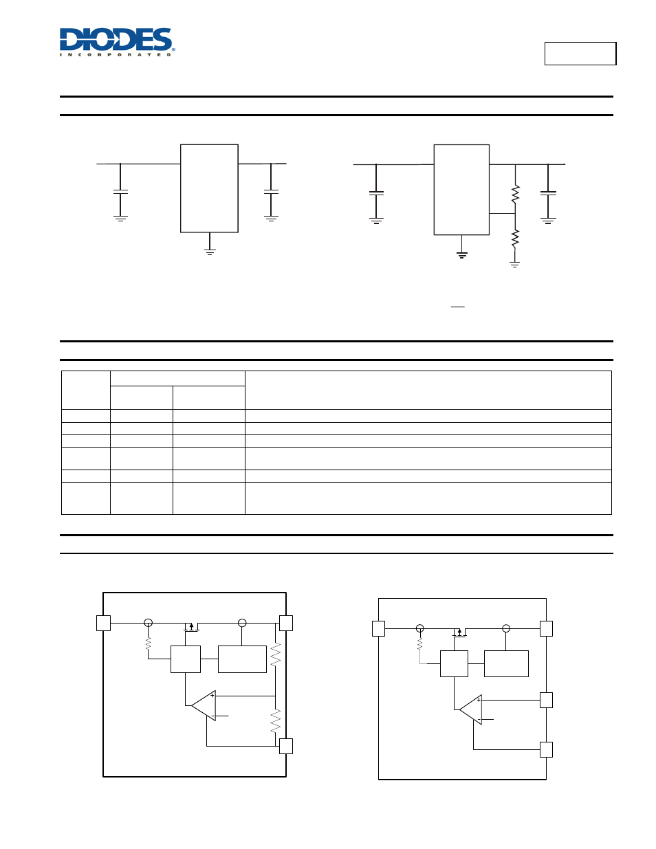
Functional Block Diagram
IN
EN
GND
OUT
Gate
Driver
0.605V
Current Limit
and Thermal
Shutdown
Fixed Version
R
R
IN
EN
GND
ADJ
OUT
Gate
Driver
0.605V
Current Limit
and Thermal
Shutdown
Adjustable Version
V
IN
V
OUT
OUT
IN
AP7363
GND
Fixed Output
10µF
10µF
V
IN
V
OUT
OUT
IN
AP7363
GND
Adjustable Output
10µF
10µF
ADJ
R2
R1