Ap7331, Electrical characteristics – Diodes AP7331 User Manual
Page 4
AP7331
300mA, LOW QUIESCENT CURRENT, FAST TRANSIENT
LOW DROPOUT LINEAR REGULATOR
AP7331
Document number: DS31914 Rev. 3 - 2
4 of 13
January 2011
© Diodes Incorporated
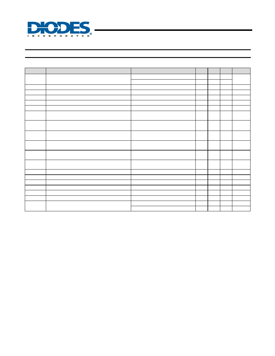
Electrical Characteristics
(T
A
= 25
o
C, V
IN
= V
OUT
+1V, C
IN
= 1uF, C
OUT
= 1uF, V
EN
= 2V, unless otherwise stated)
Symbol
Parameter
Test Conditions
Min Typ. Max
Unit
I
Q
Input Quiescent Current
V
EN
= V
IN
, I
OUT
= 0mA
⎯
55 75 μA
V
EN
= V
IN
, I
OUT
= 300mA
65
85
I
SHDN
Input Shutdown Current
V
EN
= 0V, I
OUT
= 0mA
⎯
1 μA
I
LEAK
Input Leakage Current
V
EN
= 0V, OUT grounded
⎯
1 μA
V
Dropout
Dropout Voltage (Note 4)
I
OUT
= 300mA
300
550
mV
V
REF
ADJ Reference Voltage (Adjustable version)
I
OUT
= 0mA
0.4
V
I
ADJ
ADJ Leakage (Adjustable version)
⎯
1
μA
V
OUT
Output Voltage Accuracy
T
A
= -40
o
C to 85
o
C,
I
OUT
= 30mA
-2 2 %
ΔV
OUT
/
ΔV
IN
/V
Line Regulation
V
IN
= (V
OUT
+1V) to V
IN-Max
,
V
EN
= V
IN
, I
OUT
= 1mA
0.01
0.20
%/V
ΔV
OUT
/V
OUT
Load Regulation
V
IN
= (V
OUT
+1V) to V
IN-Max
,
I
OUT
from 1mA to 300mA
-0.6 0.6 %
t
ST
Start-up
Time
V
EN
= 0V to 2.0V, V
OUT
= 1V,
I
OUT
= 300mA
80
μs
PSRR PSRR
V
IN
= [V
OUT
+1V]V
DC
+ 0.5V
ppAC
,
f = 100Hz, I
OUT
=30mA
65
dB
I
SHORT
Short-circuit
Current
V
IN
= V
IN-Min
to V
IN-Max
,
V
OUT
< 0.2V
100 mA
I
LIMIT
Current Limit
V
OUT
/R
OUT
= 1A
400
600
mA
V
IL
EN Input Logic Low Voltage
V
IN
= V
IN-Min
to V
IN-Max
0.4
V
V
IH
EN Input Logic High Voltage
V
IN
= V
IN-Min
to V
IN-Max
1.4
V
I
EN
EN Input Current
V
IN
= 0V or V
IN-Max
-1
1
μA
T
SHDN
Thermal Shutdown Threshold
140
°C
T
HYS
Thermal Shutdown Hysteresis
15
°C
θ
JA
Thermal Resistance Junction-to-Ambient
SOT25 (Note 5)
190
o
C/W
DFN2020-6 (Note 6)
167
o
C/W
Notes:
4. Dropout voltage is the voltage difference between the input and the output at which the output voltage drops 2% below its nominal value.
This parameter only applies to output voltages above 1.8V.
5. Test conditions for SOT25: Device mounted on FR-4 substrate PCB, with minimum recommended pad layout, 2oz copper, single sided
6. Test conditions for DFN2020-6: Device mounted on FR-4 substrate PCB, with minimum recommended pad layout, 2oz copper, double sided,
bottom layer is a copper plane.