Ap7217c – Diodes AP7217C User Manual
Page 7
AP7217C
1.25V 600mA CMOS LDO
AP7217C Rev. 3
7 of 9
OCTOBER 2009
DS31424
©
Diodes Incorporated
Application Note
Input Capacitor
A 1
µF ceramic capacitor is recommended to connect between IN
and GND pins to decouple input power supply glitch and noise.
The amount of the capacitance may be increased without limit. A
lower ESR (Equivalent Series Resistance) capacitor allows the
use of less capacitance, while higher ESR type requires more
capacitance. This input capacitor must be located as close as
possible to the device to assure input stability and less noise. For
PCB layout, a wide copper trace is required for both IN and GND.
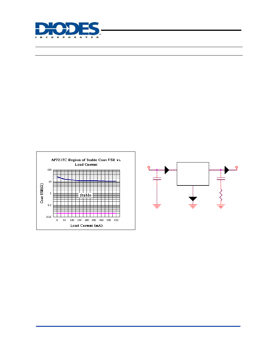
Output Capacitor
The output capacitor is required to stabilize and help the transient
response of the LDO. The AP7217C is designed to have
excellent transient response for most applications with a small
amount of output capacitance. The AP7217C is stable with any
small ceramic output capacitors of 1.0
µF or higher value, and the
temperature coefficients of X7R or X5R type. Additional
capacitance helps to reduce undershoot and overshoot during
transient. For PCB layout, the output capacitor must be placed as
close as possible to OUT and GND pins, and keep the leads as
short as possible.
ENABLE/SHUTDOWN Operation
The AP7217C (SOP-8L-EP) is turned on by setting the EN pin
high, and is turned off by pulling it low. If this feature is not used,
the EN pin should be tied to IN pin to keep the regulator output on
at all time. To ensure proper operation, the signal source used to
drive the EN pin must be able to swing above and below the
specified turn-on/off voltage thresholds listed in the Electrical
Characteristics section under V
IL
and V
IH
.
Thermal Considerations
Thermal Shutdown Protection limits power dissipation in
AP7217C. When the operation junction temperature exceeds
140°C, the Over Temperature Protection circuit starts the thermal
shutdown function and turns the pass element off. The pass
element turn on again after the junction temperature cools by
30°C. For continuous operation, do not exceed absolute
maximum operation junction temperature 125°C. The power
dissipation definition in device is:
P
D
= (V
IN
− V
OU
T) x I
OUT
+ V
IN
x I
Q
The maximum power dissipation depends on the thermal
resistance of IC package, PCB layout, the rate of surroundings
airflow and temperature difference between junctions to ambient.
The maximum power dissipation can be calculated by following
formula:
P
D(MAX)
= ( T
J(MAX)
- TA ) /
θ
JA
Where T
J(MAX)
is the maximum operation junction temperature
125°C, T
A
is the ambient temperature and the
θ
JA
is the junction
to ambient thermal resistance.
Current Limit Protection
When output current at OUT pin is higher than current limit
threshold, the current limit protection will be triggered and clamp
the output current to approximately 750mA to prevent
over-current and to protect the regulator from damage due to
overheating.
Short circuit protection
When V
OUT
pin is shorted to GND or V
OUT
voltage is less than
200mV, short circuit protection will be triggered and clamp the
output current to approximately 70mA.
Vin
Vout
C
Co
ESR
Iin
IN
AP7217C
GND
Iq
OUT
Iout