Ap7215, 600ma cmos ldo – Diodes AP7215 User Manual
Page 8
AP7215
600mA CMOS LDO
AP7215 Rev. 1
8 of 11
FEBRUARY 2009
©
Diodes Incorporated
Application Note
Input Capacitor
A 1
μF ceramic capacitor is recommended to connect between V
IN
and GND pins to decouple input power supply glitch and noise.
The amount of the capacitance may be increased without limit.
A lower ESR (Equivalent Series Resistance) capacitor allows the
use of less capacitance, while higher ESR type requires more
capacitance. This input capacitor must be located as close as
possible to the device to assure input stability and less noise. For
PCB layout, a wide copper trace is required for both V
IN
and
GND.
Suggested Input Capacitance
Vendor Capacitance
Type
Series
TAIYO YUDEN 1
μF Ceramic
LMK212B
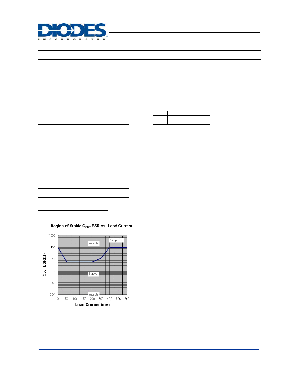
Output Capacitor
The output capacitor is required to stabilize and help the transient
response of the LDO. The AP7215 is designed to have excellent
transient response for most applications with a small amount of
output capacitance. The AP7215 is stable with any small ceramic
output capacitors of 1.0
μF or higher value, and the temperature
coefficients of X7R or X5R type. Additional capacitance helps to
reduce undershoot and overshoot during transient. For
PCB layout, the output capacitor must be placed as close as
possible to VR
OUT
and GND pins, and keep the leads as short as
possible.
Suggested Output Capacitance
Vendor Capacitance
Type
Series
TAIYO YUDEN 1
μF Ceramic
LMK212B
Suggested Resistance
Vendor Capacitance
Type
YAGEO SMD FR-SK
ENABLE/SHUTDOWN Operation
The AP7215 is turned on by setting the EN pin high, and is turned
off by pulling it low. If this feature is not used, the EN pin should
be tied to V
IN
pin to keep the regulator output on at all time. To
ensure proper operation, the signal source used to drive the
EN pin must be able to swing above and below the specified
turn-on/off voltage thresholds listed in the Electrical
Characteristics section under V
EH
and V
EL
.
Current Limit Protection
When output current at VR
OUT
pin is higher than current limit
threshold, the current limit protection will be triggered and clamp
the output current to approximately 750mA to prevent
over-current and protect the regulator from damage due to
overheating.
Short circuit protection
When VR
OUT
pin is shorted to GND or VR
OUT
voltage is less than
200mV, short circuit protection will be triggered and clamp the
output current to approximately 50mA.
VD
OUT
(reset output)
---Open-Drain Active-Low reset output---
In general, VD
OUT
is pulled up by a resistor (100K
Ω) to V
IN
. The
AP7215 microprocessor (
μP) supervisory circuitry asserts a
guaranteed logic-low reset during power-up and power-down.
Reset is asserted when V
IN
is below the reset threshold and
remain asserted for at least t
RP
after V
IN
rises above the reset
threshold.
As long as V
IN
is lower than the reset threshold, VD
OUT
remains at
logic "0". When V
IN
becomes higher than V
HYS
, a logic "1" is
asserted after a 20ms time delay defined by t
RP
VR
OUT
VD
OUT
EN=0 0V
Φ
EN=1 3.3V
Φ