Ap7165, 600ma low dropout regulator with pok, Electrical characteristics – Diodes AP7165 User Manual
Page 4
AP7165
600mA LOW DROPOUT REGULATOR WITH POK
AP7165
Document number: DS31270 Rev. 7 - 2
4 of 15
www.diodes.com
March 2012
© Diodes Incorporated
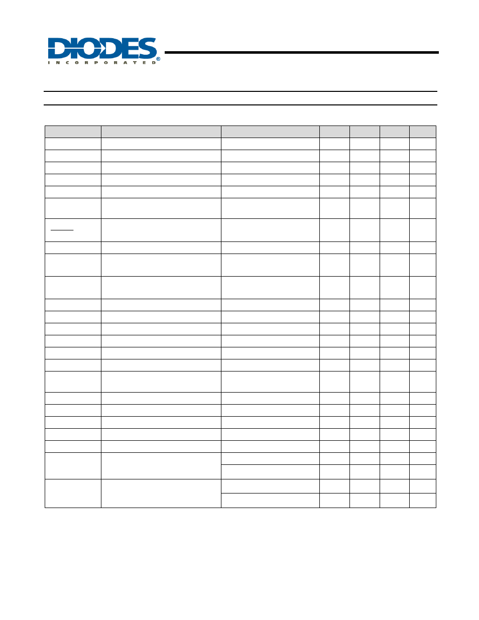
Electrical Characteristics
(T
A
= 25
o
C, V
IN
= V
OUT
+1V, C
IN
= 1µF, C
OUT
= 10µF, V
EN
= V
IN
, unless otherwise stated)
Symbol
Parameter
Test Conditions
Min
Typ.
Max
Unit
I
Q
Input Quiescent Current
I
OUT
= 0
⎯ 125 170 µA
I
SHDN
Input Shutdown Current
V
EN
= 0V, I
OUT
= 0 (Note 3)
-1 0.01 +1 µA
V
ROPOUT
Dropout Voltage
V
OUT
≥ 1.5V, I
OU T
= 500mA
300
400
mV
V
REF
FB reference voltage
0.8
V
I
FB
FB leakage
⎯ 0.01 1 µA
V
OUT
Output Voltage Total Accuracy
Over line, load and
temperature
-2.5 +2.5
%
OUT
IN
OUT
V
ΔV
ΔV
/
Line Regulation
V
IN
= V
OUT
+1V to 5.5V,
I
OUT
= 1mA
0.015 %/V
ΔV
OUT
/ V
OUT
Load Regulation
I
OUT
from 1mA to 500mA
-1.0 +1.0
%
t
ST
Start-up Time, from EN high to POK
high
V
EN
= 0V to 2.0V,
I
OUT
= 100mA, V
IN
= 3.3V
170 µs
PSRR
Power Supply Rejection Ratio
1kHz, V
IN
= 3.3V,
V
OUT
= 1.2V, I
OUT
= 0mA
60 dB
I
LIMIT
Current limit
V
OUT
= 1.8V, R
OUT
= 0.5
Ω
600 950 mA
I
SHORT
Short-circuit Current
V
IN
= 3.3V, V
OUT
< 0.2V
380 mA
V
IL
EN Input Logic Low Voltage
0.4
V
V
IH
EN Input Logic High Voltage
1.4
V
I
EN
EN Input leakage
V
EN
= 0V or 5.5V
⎯ 0.01 1 µA
V
OL
POK output low voltage
Force 2mA
100
200
mV
V
POK_TH_UP
Output voltage (rising) POK threshold
FB (or OUT for fixed version)
rising
87% 92% 97% V
ref
V
POK_Hys
Output voltage POK hysteresis
4%
V
ref
POK deglitch
V
IN
= 3.3V, V
OUT
= 1.2V
150 µs
I
POK_LK
POK leakage current
V
POK
= 5.5V
⎯ 0.01 1 µA
T
SHDN
Thermal shutdown threshold
150
°C
T
HYS
Thermal shutdown hysteresis
25
°C
θ
JA
Thermal Resistance Junction-to-
Ambient
U-DFN3030-10 (Note 4)
40
o
C/W
SO-8EP (Note 5)
27
o
C/W
θ
JC
Thermal Resistance
Junction-to- Case
U-DFN3030-10 (Note 4)
9
o
C/W
SO-8EP (Note 5)
4
o
C/W
Notes:
3. POK pin must be disconnected from IN pin.
4. Test condition for U-DFN3030-10: Device mounted on FR-4 2-layer board, 2oz copper, with minimum recommended pad on top layer and 6 vias to
bottom layer 1.0”x1.5” ground plane.
5. Test condition for SO-8EP: Device mounted on 2" x 2" FR-4 substrate PCB, 2oz copper, with minimum recommended pad on top layer and
thermal vias to bottom layer ground plane.