Ap7168, 2a low dropout regulator with pok, New prod uc t pin descriptions – Diodes AP7168 User Manual
Page 2: Functional block diagram, Absolute maximum ratings, Recommended operating conditions
AP7168
1.2A LOW DROPOUT REGULATOR WITH POK
AP7168
Document number: DS32019 Rev. 2 - 2
2 of 11
September 2010
© Diodes Incorporated
NEW PROD
UC
T
Pin Descriptions
Name
Pin Number
Description
IN
1
Voltage input pins, to be tied together externally. Bypass to ground through at least 1µF capacitor.
POK
2
Power-OK output, active-high open-drain.
EN
4
Enable input, active high.
GND 5
Ground.
FB 7
Output
feedback.
OUT 8
Voltage output pins, to be tied together externally. Bypass to ground through at least 4.7µF
ceramic capacitor.
NC
3, 6
No connection.
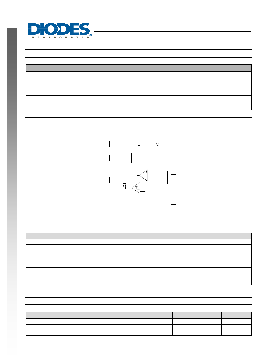
Functional Block Diagram
IN
EN
GND
FB
OUT
Gate
Driver
0.8V
0.744V
POK
Current Limit
and Thermal
Shutdown
Absolute Maximum Ratings
Symbol
Parameter
Ratings
Unit
ESD HBM
Human Body Model ESD Protection
4
KV
ESD MM
Machine Model ESD Protection
300
V
V
IN
Input
Voltage
7
V
OUT, FB, POK, EN Voltage
V
IN
+ 0.3
V
Continuous Load Current
Internal Limited
T
J
Operating Junction Temperature Range
-40 ~ 150
°C
T
ST
Storage Temperature Range
-65 ~150
°C
P
D
Power Dissipation
SO-8EP (Note 2, 4)
4.0
W
Notes: 2. Ratings apply to ambient temperature at 25°C
Recommended Operating Conditions
Symbol
Parameter
Min
Max
Unit
V
IN
Input voltage
2.2
5.5
V
I
OUT
Output Current
0
1.2
A
T
A
Operating Ambient Temperature
-40
85
°C