Data sheet, Recommended operating conditions – Diodes AP2122 User Manual
Page 5
Data Sheet
5
May. 2010 Rev. 1. 5
BCD Semiconductor Manufacturing Limited
HIGH SPEED, EXTREMELY LOW NOISE LDO REGULATOR AP2122
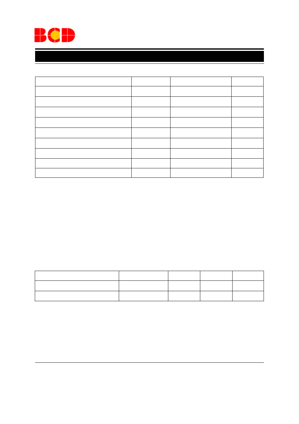
Parameter
Symbol
Value
Unit
Input Voltage
V
IN
6.5
V
Enable Input Voltage
V
CE
-0.3 to V
IN
+0.3
V
Output Current
I
OUT
300
mA
Junction Temperature
T
J
150
o
C
Storage Temperature Range
T
STG
-65 to 150
o
C
Lead Temperature (Soldering, 10sec)
T
LEAD
260
o
C
Thermal Resistance (Note 2)
θ
JA
250
o
C/W
ESD (Human Body Model)
ESD
2000
V
ESD (Machine Model)
ESD
200
V
Absolute Maximum Ratings (Note 1)
Parameter
Symbol
Min
Max
Unit
Input Voltage
V
IN
2
6
V
Operating Junction Temperature Range
T
J
-40
85
o
C
Recommended Operating Conditions
Note 1: Stresses greater than those listed under "Absolute Maximum Ratings" may cause permanent damage to the device.
These are stress ratings only, and functional operation of the device at these or any other conditions beyond those indicated
under "Recommended Operating Conditions" is not implied. Exposure to "Absolute Maximum Ratings" for extended periods
may affect device reliability.
Note 2: Absolute maximum ratings indicate limits beyond which damage to the component may occur. Electrical specifica-
tions do not apply when operating the device outside of its operating ratings. The maximum allowable power dissipation is a
function of the maximum junction temperature, T
J(max),
the junction-to-ambient thermal resistance,
θ
JA,
and the ambient tem-
perature, T
A.
The maximum allowable power dissipation at any ambient temperature is calculated using: P
D(max)
=(T
J(max)
-
T
A
)/
θ
JA.
Exceeding the maximum allowable power dissipation will result in excessive die temperature.