Data sheet, Electrical characteristics (continued) – Diodes AP2111 User Manual
Page 11
Data Sheet
600mA CMOS LDO REGULATOR WITH ENABLE AP2111
Dec. 2012 Rev. 1. 7 BCD Semiconductor Manufacturing Limited
11
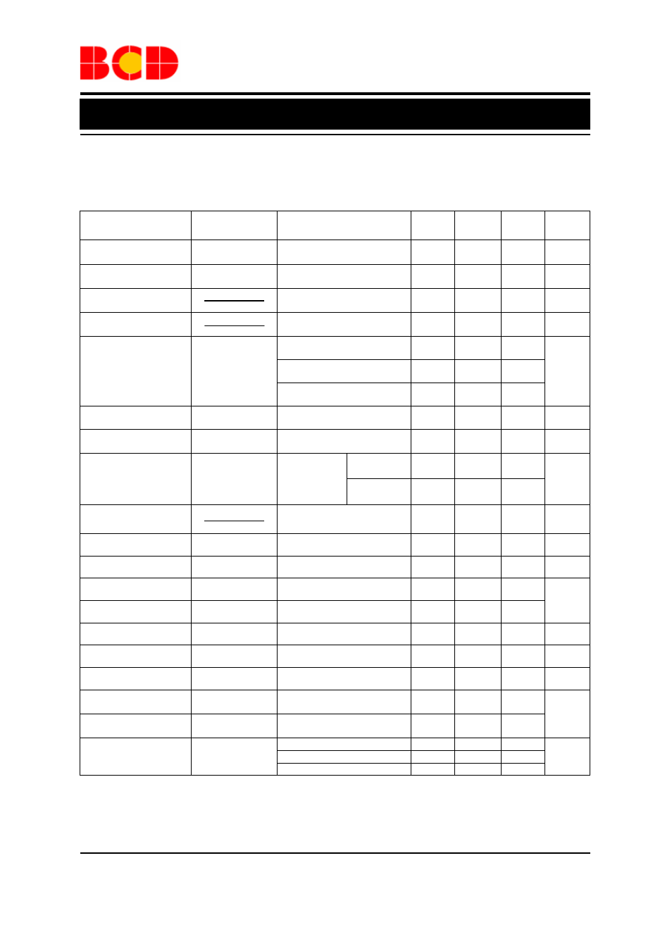
Electrical Characteristics (Continued)
AP2111-3.3 Electrical Characteristic (Note 2)
V
IN
=4.3V, C
IN
=1
μF (Ceramic), C
OUT
=1
μF (Ceramic), Typical T
A
=25°C, Bold typeface applies over -40°C≤T
A
≤85°C ranges,
unless otherwise specified (Note 3).
Note 2: To prevent the short circuit current protection feature from being prematurely activated, the input voltage
must be applied before a current source load is applied.
Note 3: Production testing at
T
A
=25
°C
. Over temperature specifications guaranteed by design only.
Parameter Symbol
Conditions Min
Typ
Max
Unit
Output Voltage
V
OUT
V
IN
=4.3V, 1mA ≤ I
OUT
≤ 30mA
V
OUT
×98.5%
3.3
V
OUT
×101.5%
V
Maximum Output Current
I
OUT(Max)
V
IN
=4.3V, V
OUT
=3.251V to
3.350V
600 mA
Load Regulation
( V
△
OUT
/V
OUT
)
△
I
OUT
V
IN
=4.3V, 1mA ≤ I
OUT
≤600mA
0.2 %/A
Line Regulation
( V
△
OUT
/V
OUT
)
△
V
IN
4.3V≤V
IN
≤6V, I
OUT
=30mA
0.02
%/V
Dropout Voltage
V
DROP
I
OUT
=10mA
5
8
mV
I
OUT
=300mA
125
200
I
OUT
=600mA
250
400
Quiescent Current
I
Q
V
IN
=4.3V, I
OUT
=0mA
55
80
μA
Standby Current
I
STD
V
IN
=4.3V, V
EN
in OFF mode
0.01
1.0
μA
Power Supply Rejection
Ratio
PSRR
Ripple 0.5Vp-p
V
IN
=4.3V,
I
OUT
=100mA
f=100Hz 65
dB
f=1kHz
65
Output Voltage
Temperature Coefficient
( V
△
OUT
/V
OUT
)
T
△
I
OUT
=30mA
T
A
=-40°C to 85°C
±100
ppm/°C
Short Current Limit
I
SHORT
V
OUT
=0V
50
mA
RMS Output Noise
V
NOISE
No Load, 10Hz ≤ f ≤100kHz 50
μV
RMS
VEN High Voltage
V
IH
Enable logic high, regulator on
1.5
6.0
V
VEN Low Voltage
V
IL
Enable logic low, regulator off
0
0.4
Start-up Time
t
S
No Load
20
μs
EN Pull Down Resistor
R
PD
3.0 m
Ω
VOUT Discharge Resistor
R
DCHG
Set EN pin at Low
60
Ω
Thermal Shutdown
Temperature
T
OTSD
160
°C
Thermal Shutdown
Hysteresis
T
HYOTSD
30
Thermal Resistance
(Junction to Case)
θ
JC
SOIC-8
74.6
°C /W
PSOP-8
43.7
SOT-223
50.9