Preliminary datasheet, Electrical characteristics, Parameter symbol condition min typ max unit – Diodes AP2822 User Manual
Page 9
Preliminary Datasheet
0.5A to 2.0A High-side Power Distribution Switches AP2822
Dec. 2012 Rev 1. 1 BCD Semiconductor Manufacturing Limited
9
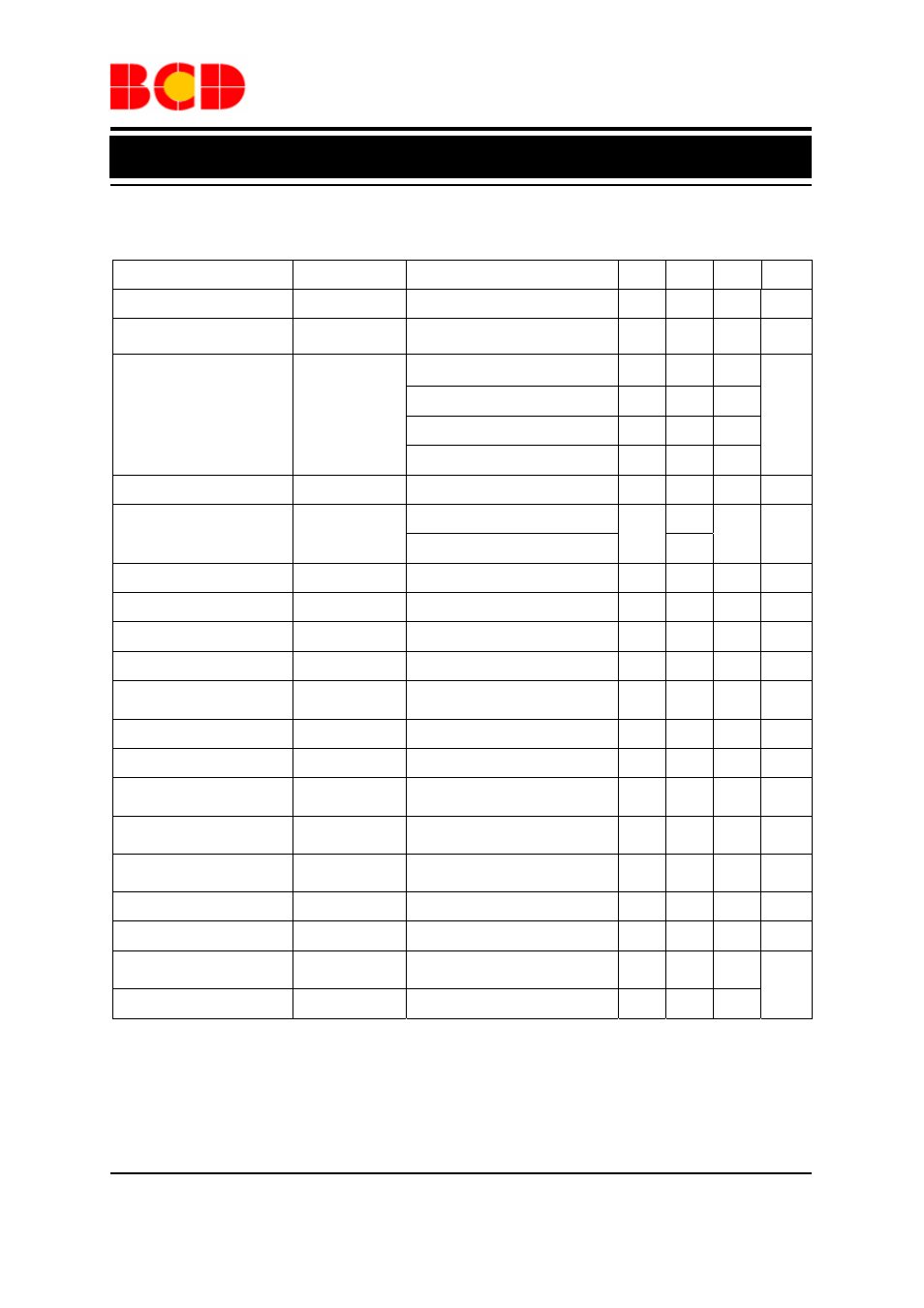
Electrical Characteristics
(V
IN
=5.0V, C
IN
=2.2µF, C
OUT
=1.0µF, Typical T
A
=25°C, unless otherwise specified)
Parameter Symbol
Condition
Min
Typ
Max
Unit
Supply Voltage
V
IN
2.7 5.5 V
Switch On Resistance
R
DS(ON)
V
IN
=5.0V, I
OUT
=2.0A
85
110
mΩ
Current Limit
I
LIMIT
AP2822A/B(0.5A) , V
OUT
=4.0V 0.7
1.0
1.4
A
AP2822C/D(1.0A), V
OUT
=4.0V 1.1
1.5
2.1
AP2822E/F(1.5A), V
OUT
=4.0V 1.65
2.2
2.8
AP2822G/H(2.0A), V
OUT
=4.0V 2.2
2.7
3.2
Supply Current
I
SUPPLY
V
IN
=5.0V, No Load
68
95
µA
Fold-back Short Current
I
SHORT
AP2822 A/B/C/D, V
OUT
=0V
0.7
A
AP2822 E/F/G/H, V
OUT
=0V 1.1
Shutdown Supply Current
I
SHUTDOWN
Chip Disable, Shutdown Mode
0.1
1.0
µA
Enable High Input Threshold
V
ENH
1.6 5.5 V
Enable Low Input Threshold
V
ENL
0 1.0 V
Enable Pin Input Current
I
EN
Force 0V to 5.0V at EN Pin
-1.0
1.0
µA
Under Voltage Lockout
Threshold Voltage
V
UVLO
V
IN
Increasing from 0V
2.2
2.5
3.0
V
Under Voltage Hysteresis
V
UVLOHY
0.2 V
Reverse Current
I
REVERSE
Chip
Disable,
V
OUT
>V
IN
0.1
1.0
µA
Output Pull Low Resistance
after Shutdown
R
DISCHARGE
100
200 Ω
Output Turn-on Time
t
ON
From Enable Active to 90% of
Output
500 µs
FLAG Pin Delay Time
t
DFLG
From Over Current Fault Condition
to Flag Active
5 10 15 ms
FLAG Pin Low Voltage
V
FLG
I
SINK
=5.0mA
35
70
mV
FLAG Pin Leakage Current
I
LEAKAGE
FLAG Disable, Force 5.0V
1.0
µA
Thermal Shutdown
Temperature
T
OTSD
150
o
C
Thermal Shutdown Hysteresis
T
HYOTSD
30