Ap1084, Electrical characteristics – Diodes AP1084 User Manual
Page 5
AP1084
5A LOW DROPOUT POSITIVE ADJUSTABLE OR
FIXED-MODE REGULATOR
AP1084 Rev. 9
5 of 11
JANUARY 2010
DS31070
©
Diodes Incorporated
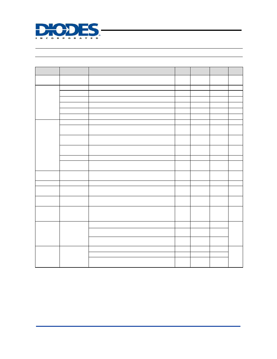
Electrical Characteristics
(Under Operating Conditions)
Symbol
Parameter
Conditions
Min
Typ.
Max
Unit
V
REF
Reference
Voltage
Io = 10mA,
T
A
= 25
o
C, (V
IN
-V
OUT
) = 1.5V
1.225
1.250 1.275 V
Line
Regulation
AP1084-XXX I
O
= 10mA, V
OUT
+1.5V IN <12V, T A = 25 o C 0.2 % AP1084-1.5 I OUT = 10mA, T A = 25 o C, 3V≦V IN ≦12V 1.470 1.500 1.530 V AP1084-1.8 I OUT = 10mA, T A = 25 o C, 3.3V≦V IN ≦12V 1.764 1.800 1.836 V AP1084-2.5 I OUT = 10mA, T A = 25 o C, 4V≦V IN ≦12V 2.450 2.500 2.550 V AP1084-3.3 I OUT = 10mA, T A = 25 o C, 4.8V≦V IN ≦12V 3.235 3.300 3.365 V AP1084-5.0 I OUT = 10mA, T A = 25 o C, 6.5V≦V IN ≦12V 4.900 5.000 5.100 V Load Regulation AP1084-Adj V IN = 3.3V, 0mA T A = 25 o C 1 % AP1084-1.5 V IN = 3V, 0mA T A = 25 o C (Note 3, 4) 12 15 mV AP1084-1.8 V IN = 3.3V, 0mA T A = 25 o C (Note 3, 4) 15 18 mV AP1084-2.5 V IN = 4V, 0mA < Io < 5A T A = 25 o C (Note 3, 4) 20 25 mV AP1084-3.3 V IN = 5V, 0mA < Io < 5A, T A = 25 o C (Note 3, 4) 26 33 mV AP1084-5.0 V IN = 8V, 0mA < Io < 5A, T A = 25 o C (Note 3, 4) 40 50 mV ΔVo Dropout I o = 5.0A ( ΔV OUT = 1% V OUT ) 1.3 1.4 V Current Limit V IN -V OUT = 5V 5.1 A Minimum Load 5 10 mA Temperature I o = 10mA 0.5 % T SD Thermal 150 O C θ JA Thermal TO220-3L 78 O C/W TO252-3L 73 TO263-3L 60 θ JC Thermal TO220-3L:Control Circuitry/Power Transistor 3.5 O C/W TO252-3L:Control Circuitry/Power Transistor 12 TO263-3L:Control Circuitry/Power Transistor 3.5 Notes: 3. See thermal regulation specifications for changes in output voltage due to heating effects. Line and load regulation are measured at a constant junction temperature by low duty cycle pulse testing. Load regulation is measured at the output lead = 1/18” from the package. recommended pay layout, no air flow. The case point of θ JC is located on the thermal tab.
Voltage
Current
Stability
Shutdown
Temperature
Resistance
Junction-to-
Ambient
(Note 5)
Resistance
Junction-to-
Case (Note 5)
4. Line and load regulation are guaranteed up to the maximum power dissipation of 15W. Power dissipation is determined by the difference
between input and output and the output current. Guaranteed maximum power dissipation will not be available over the full input/output range.
5. Test conditions for TO220-3L, TO252-3L and TO263-3L: Devices mounted on FR-4 substrate, single sided PC board, 2oz copper, with minimum