Ap2337, 0a single channel current-limited load switch, New prod uc t recommended operating conditions – Diodes AP2337 User Manual
Page 3: Electrical characteristics
AP2337
1.0A SINGLE CHANNEL CURRENT-LIMITED LOAD SWITCH
AP2337
Document number: DS35060 Rev. 2 - 2
3 of 10
October 2011
© Diodes Incorporated
NEW PROD
UC
T
Recommended Operating Conditions
Symbol
Parameter
Min
Max
Units
V
IN
Input voltage
2.7
5.5
V
I
OUT
Output Current
0
1.0
A
T
A
Operating Ambient Temperature -40
85
°C
Electrical Characteristics
(T
A
= 25
o
C, V
IN
= +5.0V, unless otherwise stated)
Symbol
Parameter
Test Conditions (Note 3)
Min
Typ.
Max Unit
V
UVLO
Input UVLO
V
IN
rising
2.00 2.65
V
I
Q
Input quiescent current
Above UVLO, I
OUT
= 0
65
110
μA
I
REV
Reverse leakage current
V
IN
= 0V, V
OUT
= 5V, I
REV
at V
IN
0.01
0.1
μA
R
DS(ON)
Switch on-resistance
V
IN
= 5V, I
OUT
= 1A
110
140
m
Ω
V
IN
= 3.3V, I
OUT
= 1A
140
170
I
LIMIT
Over-load current limit
V
IN
= 5V, V
OUT
= 4V, C
L
=10
μF
1.1 1.5 1.9 A
I
OS
Short-circuit current
OUT connected to ground, C
L
=10
μF
0.2 0.6 1.0 A
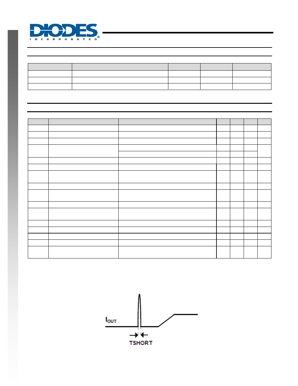
T
SHORT
Short-circuit response time
From V
OUT
< 0.6V to I
OUT
= 0A (OUT shorted to
GND) (See Figure. 1)(Note 7)
5
μs
I
ROCP
Reverse current limit
Above UVLO
0.3 0.5 0.7 A
T
Trig
Deglitch time from reverse current
trigger to MOSFET turn off
0.6 ms
V
OVP
Output over-voltage trip point
Above UVLO (Note 4)
110%
120%
V
IN
T
OVP
Debounce time from output over-
voltage to MOSFET turn off
15
μs
T
ON
Output turn-on time (Note 5)
C
L
= 1
μF, R
load
= 5
Ω (UVLO to 90% V
OUT-NOM
)
1 4
ms
T
DIS
Discharge time
C
L
= 1
μF, from UVLO to V
OUT
< 0.3V
500
μs
T
SHDN
Thermal shutdown threshold
150
°C
T
HYS
Thermal shutdown hysteresis
20
°C
θ
JA
Thermal Resistance Junction-to-
Ambient
(Note 6)
180
o
C/W
Notes:
3. Pulse-testing techniques maintain junction temperature close to ambient temperature; thermal effects must be taken into account separately.
4. During output over-voltage protection, the output draws approximately 60µA current.
5. Since the output turn-on slew rate is dependent on input supply slew rate, this limit is only applicable for input supply slew rate between 5V/0.2ms to
5V/1ms.
6. Device mounted on FR-4 substrate PCB, 2oz copper, with minimum recommended pad layout.
7. Applicable for output voltage slew rate
≤ 5V/30μs.
Figure 1. Short Circuit Response Time